SLUSG59 February   2026 BQ27Z855

ADVANCE INFORMATION  

  1.   1
  2. 1 Features
  3. 2 Applications
  4. 3 Description
  5. 4 Pin Configurations and Functions
  6. 5 Specifications
    1. 5.1  Absolute Maximum Ratings
    2. 5.2  ESD Ratings
    3. 5.3  Recommended Operating Conditions
    4. 5.4  Supply Current
    5. 5.5  1.8V LDO Regulator (REG18)
    6. 5.6  Low Frequency Oscillator (LFO)
    7. 5.7  High Frequency Oscillator (HFO)
    8. 5.8  PACK Clamp (PACK_CLAMP)
    9. 5.9  Analog-to-Digital Converter (VADC)
    10. 5.10 Coulomb Counter (CCADC)
    11. 5.11 Coulomb Counter Digital Filter (CC1)
    12. 5.12 Current Measurement Digital Filter (CC2)
    13. 5.13 Charge Current Measurement Digital Filter (CC3)
    14. 5.14 Wake-up Comparator (I-WAKE)
    15. 5.15 Internal Temperature Sensor (INT_TEMP)
    16. 5.16 Thermistor Measurement Support
    17. 5.17 Hardware-based Protection (SCOMP) Thresholds (OVP, UVP, OCC, OCD, SCD)
    18. 5.18 Hardware-based Protections (SCOMP) Timing (OVP, UVP, OCC, OCD, SCD)
    19. 5.19 Current Limiter
    20. 5.20 CHG, DSG NFET Drivers
    21. 5.21 Zero-volt Charging (ZVCHG)
    22. 5.22 General Purpose Input-Outputs (INT)
    23. 5.23 I2C Interface I/O (SDA, SCL)
    24. 5.24 I2C Interface Timing
  7. 6 Detailed Description
    1. 6.1 Overview
    2. 6.2 Functional Block Diagram
    3. 6.3 Feature Description
      1. 6.3.1  BQ27Z855 Processor
      2. 6.3.2  Battery Parameter Measurements
        1. 6.3.2.1 Analog-to-Digital Converter (VADC)
        2. 6.3.2.2 VADC Multiplexer
        3. 6.3.2.3 Coulomb Counter (CCADC) and Digital Filter (CC1)
        4. 6.3.2.4 Internal Temperature Sensor (INT_TEMP)
        5. 6.3.2.5 External Temperature Sensor Support
      3. 6.3.3  Power Supply Control
      4. 6.3.4  ENAB Pin
      5. 6.3.5  I2C Bus Communication Interface
      6. 6.3.6  Low Frequency Oscillator (LFO)
      7. 6.3.7  High Frequency Oscillator (HFO)
      8. 6.3.8  Real Time Clock (RTC)
      9. 6.3.9  1.8V Low Dropout Regulator (REG18)
      10. 6.3.10 FET Drivers (CHG, DSG)
        1. 6.3.10.1 Charge (CHG) FET Driver
        2. 6.3.10.2 Discharge (DSG) FET Driver
      11. 6.3.11 Zero-volt Charging (ZVCHG)
      12. 6.3.12 Integrated Protections
        1. 6.3.12.1 Hardware-based Protections
          1. 6.3.12.1.1 Overvoltage Protection (OVP)
          2. 6.3.12.1.2 Undervoltage Protection (UVP)
          3. 6.3.12.1.3 Overcurrent in Charge Protection (OCC)
          4. 6.3.12.1.4 Overcurrent in Discharge Protection (OCD)
          5. 6.3.12.1.5 Short Circuit Current in Discharge Protection (SCD)
          6. 6.3.12.1.6 Wake-up Comparator (I-WAKE)
        2. 6.3.12.2 Firmware-based Protections
          1. 6.3.12.2.1 Primary Level Protection Features
          2. 6.3.12.2.2 Secondary Level Protection Features
      13. 6.3.13 Gas Gauging
      14. 6.3.14 Advanced Battery Algorithms
        1. 6.3.14.1 Si-anode Chemistry Support
        2. 6.3.14.2 Internal Short Indication (ISI)
        3. 6.3.14.3 Battery Swelling Detection (BSD)
      15. 6.3.15 Integrated Current Limiter and Charge Control Features
        1. 6.3.15.1 Integrated Current Limiter
          1. 6.3.15.1.1 CHG FET State Machine
          2. 6.3.15.1.2 Linear Mode
            1. 6.3.15.1.2.1 Battery Charging Process
            2. 6.3.15.1.2.2 Zero-volt Charge (ZVCHG)
            3. 6.3.15.1.2.3 Precharge (PCHG)
            4. 6.3.15.1.2.4 Fast Charge (CC)
            5. 6.3.15.1.2.5 Taper-charge (CV)
            6. 6.3.15.1.2.6 Charge Termination (VCT)
            7. 6.3.15.1.2.7 Step-charging Profile Support
          3. 6.3.15.1.3 MINSYS Mode
          4. 6.3.15.1.4 Battery Supplement Mode
        2. 6.3.15.2 Interaction with a Smart Charger
      16. 6.3.16 Ideal Diode Mode
      17. 6.3.17 Lifetime Data Logging Features
      18. 6.3.18 Authentication
        1. 6.3.18.1 ECC ECDSA Authentication
        2. 6.3.18.2 SHA-256 Authentication
      19. 6.3.19 Over the Air (OTA) Field Updater
      20. 6.3.20 Configuration
        1. 6.3.20.1 Cell Voltage Measurements
        2. 6.3.20.2 Coulomb Counting
        3. 6.3.20.3 Temperature Measurements
    4. 6.4 Device Functional Modes
  8. 7 Application and Implementation
    1. 7.1 Application Information
    2. 7.2 Typical Application Schematics
      1. 7.2.1 Design Requirements
      2. 7.2.2 Detailed Design Procedure
        1. 7.2.2.1 High-Current Path
          1. 7.2.2.1.1 Protection FETs
          2. 7.2.2.1.2 Battery Cell Connections
          3. 7.2.2.1.3 Sense Resistor
          4. 7.2.2.1.4 ESD Mitigation
        2. 7.2.2.2 Gas Gauge Circuit
          1. 7.2.2.2.1 Cell Voltage Measurement Interface
          2. 7.2.2.2.2 Coulomb Counter Interface
          3. 7.2.2.2.3 Temperature Measurement
          4. 7.2.2.2.4 1.8V Low Dropout Regulator (REG18)
          5. 7.2.2.2.5 I2C Communication (SDA, SCL)
          6. 7.2.2.2.6 Interrupt to Host Interface (INT)
        3. 7.2.2.3 Current Limiter Circuit
          1. 7.2.2.3.1 Protection FETs and Compatibility with BQ27Z855
          2. 7.2.2.3.2 CP Control Logic and Capacitor
          3. 7.2.2.3.3 Voltage-based Feedback Interface
          4. 7.2.2.3.4 Current-based Feedback Interface
            1. 7.2.2.3.4.1 Sense Resistor Impact on Current-based Feedback
            2. 7.2.2.3.4.2 Sense Resistor Impact on CHG FET State Transitions
          5. 7.2.2.3.5 BAT-PACK Dedicated Voltage Comparator (DCOMP)
            1. 7.2.2.3.5.1 Impact of Sense Resistor Configuration on DCOMP Sensing
          6. 7.2.2.3.6 System-level Recommendations
        4. 7.2.2.4 Co-design with BQ27Z746 and BQ27Z758
          1. 7.2.2.4.1 Footprint Compatibility and Equivalent Pins
          2. 7.2.2.4.2 Co-layout Example
  9. 8 Power Supply Recommendations
  10. 9 Layout
    1. 9.1 Layout Guidelines
  11. 10Device and Documentation Support
    1. 10.1 Third-Party Products Disclaimer
    2. 10.2 Documentation Support
      1. 10.2.1 Related Documentation
    3. 10.3 Trademarks
    4. 10.4 Electrostatic Discharge Caution
    5. 10.5 Glossary
  12. 11Revision History
  13. 12Mechanical, Packaging, and Orderable Information
    1.     PACKAGE OPTION ADDENDUM
    2. 12.1 Tape and Reel Information
    3. 12.2 Mechanical Data
CP Control Logic and Capacitor

To support supplement mode and consecutive high system load pulses, the device turns the CHG FET ON using internal control logic and an external capacitor (CCP) connected between the device's CP and CP_BOOT pins. This capacitor is discharged to the device's CHG pin when the device enters the CHG = LIN_ON state and is recharged immediately after the CHG FET turns ON. Additionally if the device's current limiter is enabled, the external CCP capacitor is charged during device operation regardless of whether the device is actively charging a battery.

When the external CP capacitor charges, the capacitor charges using the available battery voltage. To ensure the device properly enters and exits supplement mode, additional resistance between the positive terminal of the cell (CELL+) and the device's BAT pin is not recommended. This prevents unintended device brownouts when the CP capacitor must be recharged in between high system load pulses to support the next entry into supplement mode. The total resistance between CELL+ and the device BAT pin is not recommended to exceed 110mΩ.

Place the external CP capacitor with the recommended typical capacitance of 1µF connected between the CP and CP_BOOT pins as close to the device as possible.
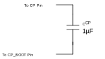
BQ27Z855 CP Capacitor Figure 7-13 CP Capacitor