SLVAE09B July 2018 – August 2021 TPS560430
2.1 Overall Control Block Diagram and Transfer Function Derivation
Figure 2-1 shows the simplified schematic for the PCM buck converter.
 Figure 2-1 Simplified Schematic for PCM Buck Converter
 Figure 2-2 Overall Control Implementation
Figure 2-2 shows the overall control block model where:
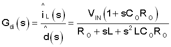
- Gdi(s) is the duty cycle to iL transfer function.
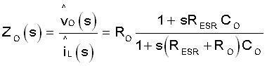
- ZO(s) is the transfer function of output impedance.
- Gdiv(s) is the gain of the feedback resistor network.
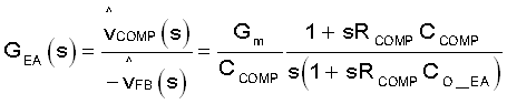
- GEA(s) is the transfer function of the error amplifier with certain compensation.
- Fm is the gain of PCM PWM comparator.
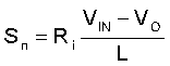
- Ri is the current sensing resistor.
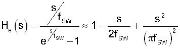
- He(s) is the transfer function model of inductor current sampling-hold effect.
Equation 1 shows the transfer function from the inductor current to the output voltage.
Gdi(s) is the duty cycle to iL transfer function.
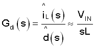
The internal loop compensation is designed so that the crossover frequency is much higher than the corner frequency, 1/(2π√LCO). For crossover frequency and higher frequency, Equation 2 can be simplified as Equation 3.
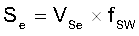
The sensed inductor current, external ramp, and the output of error amplifier VCOMP are compared, which determines when to turn off the high side MOSFET, hence the duty cycle is determined. Fm is the comparator gain. fSW is the switching frequency. Sn is the on-time slope of the sensed-current waveform and Se is the external ramp slope.
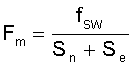
where
He(s) is the transfer function model of inductor current sampling-hold effect. [2]2:
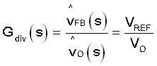
Equation 6 shows the transfer function of the feedback.
Equation 7 shows the transfer function of the error amplifier with certain compensation.