SLVAE09B July 2018 – August 2021 TPS560430
3.2 Output Capacitor Design
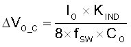
The output capacitor is designed based on output ripple and loop response. The output voltage ripple is composed of two parts. One is caused by the inductor current ripple going through the ESR of the output capacitor, see Equation 19. The other is caused by the inductor current ripple charging and discharging the output capacitor, see Equation 20. The target output ripple is 30 mV, so ΔVO_ESR < 30 mV and ΔVO_C < 30 mV, then RESR < 125 mΩ and CO > 0.91 μF.
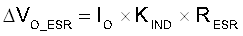
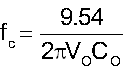
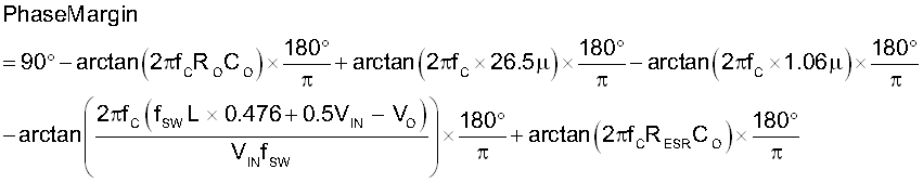
From Equation 13, the maximum ESR value is calculated to get a reasonable crossover frequency and enough phase margin. If you assume the target crossing over frequency fc is about 20 kHz, then the result is RESR ≪ 612 mΩ. Three times margin is suggested and the result is RESR < 204 mΩ.
Output capacitor value determines loop response in internally compensated PCM buck converters, as Equation 15 and Equation 16. With TPS560430 internal parameter, the calculation equation is as Equation 21 and Equation 22. The target fc is about 20 kHz, so CO is about 15 μF. Consider of derating, one 22-μF, 16-V ceramic capacitor with 4-mΩ ESR is used. The capacitance after derating is 13 μF: CO = 13 μF, RESR = 4 mΩ. The crossover frequency is fc = 23.4 kHz and the phase margin is calculated as 64.2° at VIN = 12 V, IO = 0.6 A. The equation also indicates that the worst phase margin happens at minimum VIN and minimum IO, while the calculation result is 59.2° at VIN = 7 V, IO = 0.1 A. They meet design specs.