SLVAE09B July 2018 – August 2021 TPS560430
2.2 Inside Current Loop Model
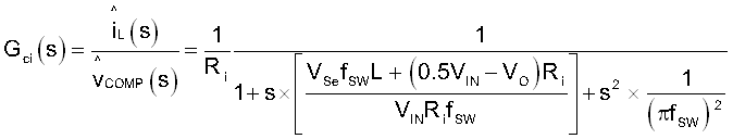
Based on Equation 3 to Equation 5 and Figure 2-2, the transfer function from control to inductor current is Gci(s):
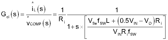
For PCM buck converter, the crossover frequency is much smaller than half switching frequency, so around crossover frequency Equation 8 can be simplified as Equation 9. The inside current loop is simplified as a single pole, which is very helpful for the loop response analysis of PCM buck converter.
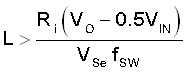
If the inside current loop Gci(s) is not stable, subharmonic oscillation occurs. A system is stable as long as each of the poles of the closed loop transfer function lies in the left half plane. The minimum inductor value is calculated to prevent subharmonic oscillation: