SLVAE09B July 2018 – August 2021 TPS560430
3.3 Simulation and Bench Verification
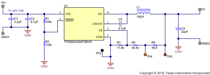
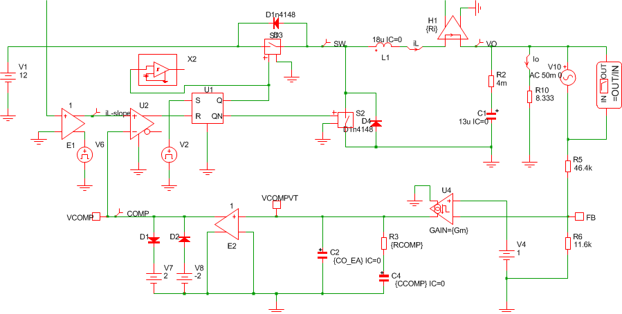
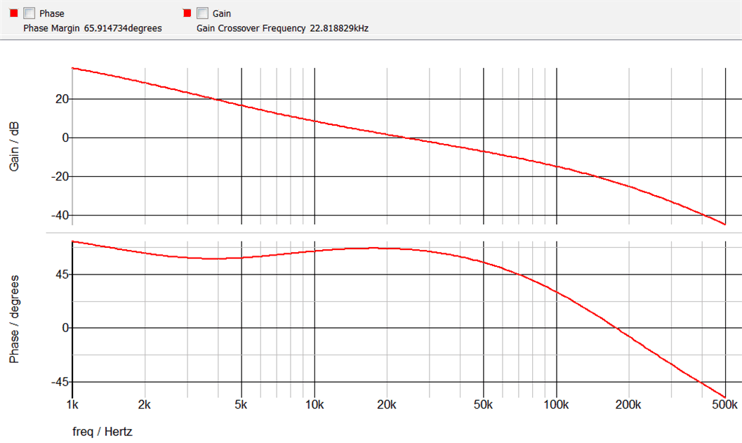
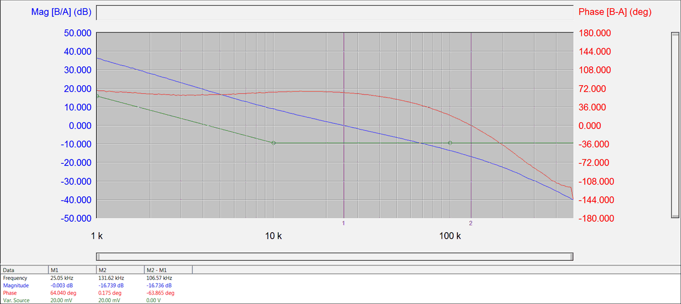
Figure 3-1 shows the schematic for bench verification. SIMPLIS is used to simulate the loop response as shown in Figure 3-2. Figure 3-3 and Figure 3-4 are the loop responses from the SIMPLIS simulation and bench test under VIN = 12 V, VO = 5 V, IO = 0.6 A, and fSW = 1.1 MHz. Table 3-2 compares the calculation results, simulation results, and bench measurement at different VIN. It can be seen that the proposed model in this application report is accurate.
 Figure 3-1 TPS560430XF Design With 5-V Output
 Figure 3-2 Schematic of A Simplified SIMPLIS Model
 Figure 3-3 Bode Plot Simulation Result at
VIN = 12 V, IO = 0.6 A
 Figure 3-4 Bode Plot Test Result at
VIN = 12 V, IO = 0.6 A
Figure 3-4 Bode Plot Test Result at
VIN = 12 V, IO = 0.6 ATable 3-2 Calculation, Simulation, and
Bench Measurement Results Comparison
| VIN (V) | IO (A) | CALCULATION RESULTS | SIMULATION RESULTS | BENCH MEASUREMENT | |||
|---|---|---|---|---|---|---|---|
| fc (kHz) | PHASE MARGIN (°) | fc (kHz) | PHASE MARGIN (°) | fc (kHz) | PHASE MARGIN (°) | ||
| 7 | 0.1 | 23.4 | 59.2 | 22.8 | 61.3 | 23.6 | 58.4 |
| 7 | 0.6 | 23.4 | 62.2 | 22.7 | 64.4 | 24.7 | 61.7 |
| 12 | 0.1 | 23.4 | 61.2 | 22.9 | 62.8 | 24.6 | 60.3 |
| 12 | 0.6 | 23.4 | 64.2 | 22.8 | 65.9 | 25.1 | 64 |
| 36 | 0.1 | 23.4 | 63 | 22.9 | 64.3 | 23.7 | 61.1 |
| 36 | 0.6 | 23.4 | 66 | 22.9 | 67.4 | 23.9 | 66.3 |