SLVAE09B July 2018 – August 2021 TPS560430
2.4 Inductor and Output Capacitor Design Limits
Figure 2-3 shows the Bode plot with proper inductor and output capacitor design. fc ≫ fP_OUT, fc ≫ fZ_EA, fc ≪ fP_EA, fc ≪ fP_ci, fc ≪ fZ_OUT
 Figure 2-3 Bode Plot Model for PCM Buck Converter
The gain curve must go across 0 dB with a -20 dB/dec slew rate, so that the phase margin is enough. The zero introduced by the compensation network fZ_EA cancels the pole of output impedance fP_OUT, and they are placed far before crossover frequency: fP_OUT ≪ fc, fZ_EA ≪ fc. The parasitic capacitor of error amplifier CO_EA is quite small, so fP_EA ≫ fc.
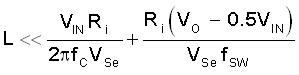
If L is too large, the pole introduced by the current loop fP_ci is smaller than the crossover frequency fc. The gain curve goes across 0 dB with a -40 dB/dec slew rate, and the phase margin is not enough. Besides, the loop response is influenced by VIN since fP_ci is influenced by VIN. To prevent that from happening, L must be properly designed to ensure fP_ci ≫ fc. Equation 12 calculates the maximum inductor value.
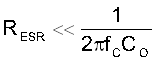
If the Equivalent Series Resistance (ESR) of output capacitor is too large, the zero introduced by the output capacitor fZ_OUT is smaller than the crossover frequency fc. The gain curve has a 0 dB/dec slew rate after fZ_OUT, which makes the crossover frequency too large. Some high frequency poles introduced by the parasitic parameters in the IC influence the phase margin, and the phase margin is not enough. To prevent that, ESR of the output capacitor must be properly designed to ensure fZ_OUT ≫ fc. Equation 13 calculates the maximum ESR.