SLVAE09B July 2018 – August 2021 TPS560430
2.3 Overall Loop Model
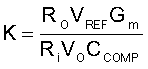
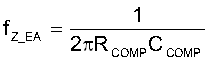
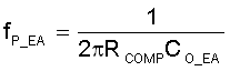
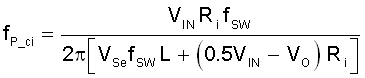
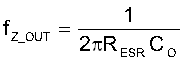
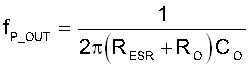
fZ_EA and fP_EA are zeros and poles introduced by the error amplifier with certain compensation. fZ_OUT and fP_OUT are zeros and poles introduced by the output capacitor and load. fP_ci is the pole introduced by the inside current loop. Based on Equation 1, Equation 6, Equation 7, and Equation 9, the open loop transfer function L(s) around crossover frequency is obtained:
Equation 11. 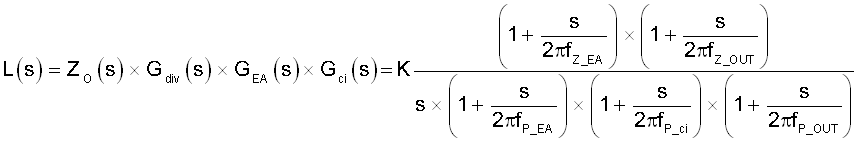
where