SNVA856B May 2020 – October 2022 LM63615-Q1 , LM63625-Q1 , LM63635-Q1 , LMR33620 , LMR33620-Q1 , LMR33630 , LMR33630-Q1 , LMR33640 , LMR36006 , LMR36015 , TPS54360B , TPS54560B
- Working With Inverting Buck-Boost Converters
- Trademarks
- 1 Introduction
- 2 Inverting Buck-Boost Converter
- 3 Basic Operation
- 4 Operating Considerations of a Buck Based Inverting Buck-Boost
- 5 Component Selection for the IBB
- 6 General Considerations
- 7 Auxiliary Functions
- 8 Design Examples
- 9 Summary
- 10References
- 11Revision History
2 Inverting Buck-Boost Converter
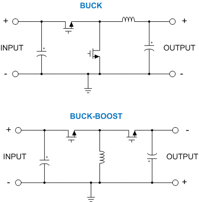
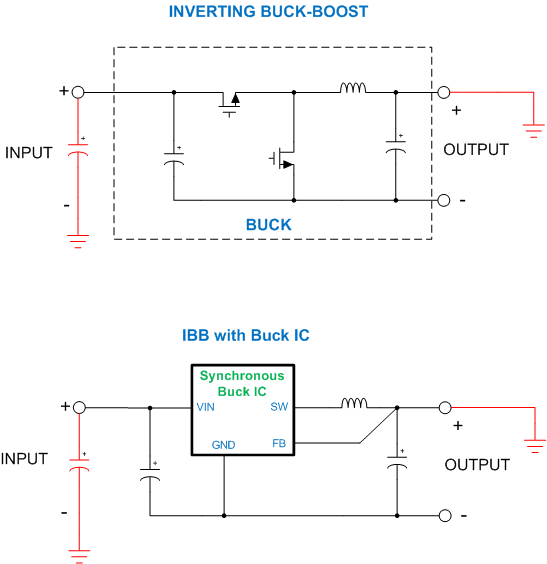
The diagrams in Figure 2-1 show a comparison between an ordinary buck DC/DC converter and the IBB. The buck converter takes a positive input voltage and converts it to a positive output voltage of smaller magnitude. The IBB takes a positive input voltage and coverts it to a negative output voltage, with a common ground connection between input and output. It is easy to see the similarity between the two converters. The top schematic in Figure 2-2 shows the connections for taking the buck regulator and converting it into an IBB. Looking at the connections shown in red, we see that the buck output is now the system ground and the buck "ground" becomes the negative output. An additional input capacitor is added between the input supply and system ground. The lower schematic shows the connections when using a synchronous buck regulator IC. A non-synchronous converter can also be used. Notice that the "ground" reference for the IC is now the negative output voltage. This has consequences for the maximum input voltage and the control inputs when using this configuration. Also, notice that the feed-back connection to the regulator is not changed from that of an ordinary buck. Although the examples show a synchronous buck with an internal feedback divider, a non-synchronous IC, and/or external feedback dividers can also be used.
The connection changes are detailed in the following list:
- Reassign buck positive output as system ground.
- Reassign buck regulator ground nodes as the negative output voltage node.
- Positive input stays the same.
 Figure 2-1 Comparison of Buck and Inverting Buck-Boost Topology
 Figure 2-2 Converting a Buck to an Inverting Buck-Boost