SNVA856B May 2020 – October 2022 LM63615-Q1 , LM63625-Q1 , LM63635-Q1 , LMR33620 , LMR33620-Q1 , LMR33630 , LMR33630-Q1 , LMR33640 , LMR36006 , LMR36015 , TPS54360B , TPS54560B
- Working With Inverting Buck-Boost Converters
- Trademarks
- 1 Introduction
- 2 Inverting Buck-Boost Converter
- 3 Basic Operation
- 4 Operating Considerations of a Buck Based Inverting Buck-Boost
- 5 Component Selection for the IBB
- 6 General Considerations
- 7 Auxiliary Functions
- 8 Design Examples
- 9 Summary
- 10References
- 11Revision History
3 Basic Operation
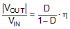
The basic operation of the converter is shown in Figure 3-1. During the portion of the switching cycle in which the HS FET is on, the inductor voltage is equal to VIN. For the remainder of the switching cycle, the LS FET turns on and the inductor voltage is -VOUT. At this point the inductor energy is supplied to the load and the output capacitor. The controller regulates the output voltage by adjusting the duty cycle of the HS and LS FET switches. Performing a standard analysis on the circuit in Figure 3-1, we arrive at the conversion law found in Equation 1.
where
- η = Efficiency
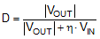
A plot of this equation is shown in Figure 3-2 for a typical duty cycle range of 0.1 to 0.9. The first thing to notice is that the conversion ratio can be less than or greater than one. This means that the IBB can either increase or decrease the input voltage, depending on the duty cycle D; hence the name "buck-boost". For example you can regulate to an output voltage of –5 V from an input voltage of from 5 V and 24 V or convert an input range of 12 V to 24 V to an output of –15 V. The controller smoothly moves from "buck" mode to "boost" mode as the input voltage changes, while regulating the output voltage. Rearranging Equation 1, we arrive at the duty cycle as a function of our input and output voltages; as found in Equation 2.
In the IBB topology, both the input and output currents are "chopped". In other words these currents are discontinuous and have very fast transition times. This means that the IBB may generate more voltage spikes in the output voltage than a buck. These issues can be addressed with properly sized output capacitors or post regulation filters.
 Figure 3-1 Inverting Buck-Boost Waveforms
 Figure 3-2 Conversion Ratio vs Duty Cycle