SNVA856B May 2020 – October 2022 LM63615-Q1 , LM63625-Q1 , LM63635-Q1 , LMR33620 , LMR33620-Q1 , LMR33630 , LMR33630-Q1 , LMR33640 , LMR36006 , LMR36015 , TPS54360B , TPS54560B
- Working With Inverting Buck-Boost Converters
- Trademarks
- 1 Introduction
- 2 Inverting Buck-Boost Converter
- 3 Basic Operation
- 4 Operating Considerations of a Buck Based Inverting Buck-Boost
- 5 Component Selection for the IBB
- 6 General Considerations
- 7 Auxiliary Functions
- 8 Design Examples
- 9 Summary
- 10References
- 11Revision History
4.1 Voltage Stress
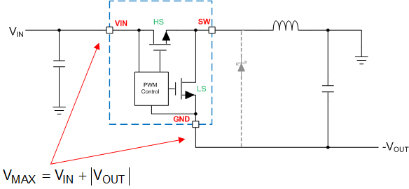
Selecting a buck regulator to convert to an IBB requires special attention to the voltage and current requirements of the application. A quick glance at Figure 4-1 shows that the voltage across the VIN and GND pins of the regulator IC is equal to the input voltage plus the negative output voltage. This voltage is greater than for a buck regulator, which only sees the input voltage across the VIN and GND terminals. As an example, if you needed to convert from an input of +24 V to an output of –15 V, you would need a regulator with a voltage rating of at least 39 V. This would exclude many of the available "36-V" devices, requiring the use of a device rated at 40 V or more. The data sheet specification that applies here is the "Input Voltage Absolute Maximum" ratings. The same applies to the voltage rating of the "catch" diode in a non-synchronous solution.
 Figure 4-1 Voltage Stress on an IBB