SPRAA99C March 2008 – May 2021 AM3351 , AM3352 , AM3354 , AM3356 , AM3357 , AM3358 , AM3359 , AM4372 , AM4376 , AM4377 , AM4378 , AM4379 , OMAPL138B-EP , TMUX646
4.4 Reflow
Solder reflow conditions are the next critical step in the mounting process. During reflow, the solvent in the solder paste evaporates, the flux cleans the metal surfaces, the solder particles melt, wetting of the surfaces takes place by wicking of molten solder, the solder balls collapse, and finally solidification of the solder into a strong metallurgical bond completes the process. The desired end result is a uniform solder structure strongly bonded to both the PCB and the package with small or no voids and a smooth, even fillet at both ends. Conversely, when all the steps do not carefully fit together, voids, gaps, uneven joint thickness, discontinuities, and insufficient fillet can occur. While the exact cycle used depends on the reflow system and paste composition, there are several key points all successful cycles have in common.
The first of these is a warm-up period sufficient to safely evaporate the solvent. This can be done with a pre-heat or a bake, or, more commonly, a hold in the cycle at evaporation temperatures. If there is less solvent in the paste (such as in a high-viscosity, high-metal-content paste), then the hold can be shorter. However, when the hold is not long enough to get all of the solvent out or too fast to allow it to evaporate, many negative things happen. These range from solder-particle splatter to trapped gases, which can cause voids and embrittlement. A significant number of reliability problems with solder joints can be solved with the warm-up step, so it needs careful attention.
The second key point that successful reflow cycles have in common is uniform heating across the package and the board. Uneven solder thickness and non-uniform solder joints may be an indicator that the profile needs adjustment. There can also be a problem when different sized components are reflowed at the same time. Care needs to be taken when profiling an oven to be sure that the indicated temperatures are representative of what the most difficult to reflow parts are seeing. These problems are more pronounced with some reflow methods, such as infrared (IR) reflow, than with others, such as forced hot-air convection.
Finally, successful reflow cycles strike a balance among temperature, timing, and length of cycle. Mistiming may lead to excessive fluxing activation, oxidation, excessive voiding, or even damage to the package. Heating the paste too hot, too quickly before it melts can also dry the paste, which leads to poor wetting. Process development is needed to optimize reflow profiles for each solder paste/flux combination.
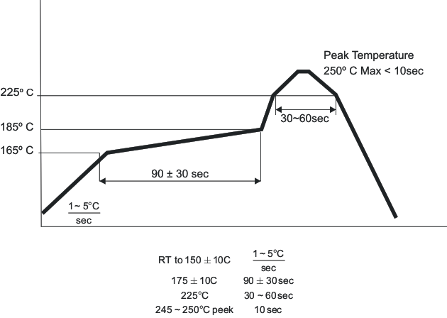
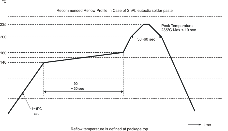
The profile shown in Figure 4-2 is an ideal one for use on a Pb-Free nFBGA package in a forced-air-convection furnace, which is the most highly recommended type. The best results have been found in a nitrogen atmosphere. The corresponding optimal reflow profile for an nFBGA package exhibiting eutectic SnPb solder balls is shown in Figure 4-3.
The guidelines upon which these profiles are based are general. Modification to the ideal reflow profile will be driven by the interplay of solder-paste particle size and flux percentage with process variables such as heating rates, peak temperatures, board construction factors, and atmosphere. These modifications are dependent on specific applications.
It should be noted that while they are more rugged than most CSP-type packages, many nFBGA packages are still slightly moisture-sensitive at the time of publishing this application report. The time out of a dry environment should be controlled according to the label on the packing material. This will prevent moisture absorption problems with the package such as “popcorning,” or delamination.
 Figure 4-2 Recommended Reflow Profile of Pb-Free nFBGA Package
 Figure 4-3 Recommended Reflow Profile of Eutectic SnPb nFBGA Package
Other concerns with BGA packages are those caused by a PCB bowing or twisting during reflow. As PCBs get thinner, these problems will become more significant. Potential problems from these effects will show up as open pins, hourglass solder joints, or solder discontinuities. Proper support of the PCB through the furnace, balancing the tab attachments to a panel, and, in worst cases, using a weight to stiffen the PCB can help prevent this. In general, the small size of CSPs create fewer problems than standard BGAs. It is also true that BGAs generally have fewer problems than leaded components.