TIDUD61E October 2020 – April 2021
- Description
- Resources
- Features
- Applications
- 5
- 1System Description
- 2System Overview
-
3Hardware, Software, Testing Requirements, and Test Results
- 3.1
Required Hardware and Software
- 3.1.1 Hardware
- 3.1.2
Software
- 3.1.2.1 Opening Project Inside CCS
- 3.1.2.2 Project Structure
- 3.1.2.3 Using CLA on C2000 MCU to Alleviate CPU Burden
- 3.1.2.4 CPU and CLA Utilization and Memory Allocation
- 3.1.2.5
Running the Project
- 3.1.2.5.1 Lab 1: Open Loop, DC (PFC Mode)
- 3.1.2.5.2 Lab 2: Closed Current Loop DC (PFC)
- 3.1.2.5.3 Lab 3: Closed Current Loop, AC (PFC)
- 3.1.2.5.4 Lab 4: Closed Voltage and Current Loop (PFC)
- 3.1.2.5.5 Lab 5: Open loop, DC (Inverter)
- 3.1.2.5.6 Lab 6: Open loop, AC (Inverter)
- 3.1.2.5.7 Lab 7: Closed Current Loop, DC (Inverter with resistive load)
- 3.1.2.5.8 Lab 8: Closed Current Loop, AC (Inverter with resistive load)
- 3.1.2.5.9 Lab 9: Closed Current Loop (Grid Connected Inverter)
- 3.1.2.6 Running Code on CLA
- 3.1.2.7
Advanced Options
- 3.1.2.7.1 Input Cap Compensation for PF Improvement Under Light Load
- 3.1.2.7.2 83
- 3.1.2.7.3 Adaptive Dead Time for Efficiency Improvements
- 3.1.2.7.4 Phase Shedding for Efficiency Improvements
- 3.1.2.7.5 Non-Linear Voltage Loop for Transient Reduction
- 3.1.2.7.6 Software Phase Locked Loop Methods: SOGI - FLL
- 3.2 Testing and Results
- 3.1
Required Hardware and Software
- 4Design Files
- 5Software Files
- 6Related Documentation
- 7About the Author
- 8Revision History
3.1.2.4 CPU and CLA Utilization and Memory Allocation
The CPU utilization can be monitored by toggling GPIOs and capturing the waveforms using oscilloscope. Each ISR includes profiling functions that set GPIO pin high at the beginning of ISR and set GPIO pin low at the end of ISR. However, this method is no longer accurate when ISRs are nested.
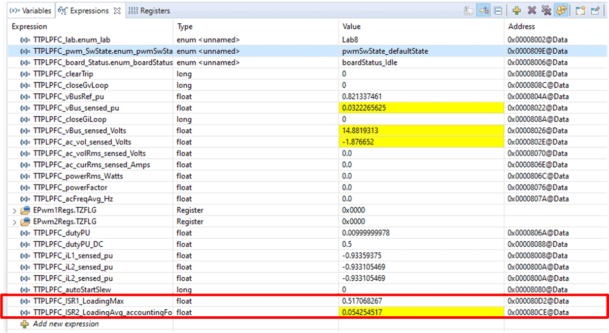
To overcome the drawback of the oscilloscope-based method, XBAR and ECAP module are utilized to capture the toggling instant of GPIOs and MCU calculates ISR loading that accommodates nesting. Furthermore, this method provides ISR loadings directly on watch window and therefore, oscilloscope is not required. ISR1(100 kHz) is designed for inner current loop control. The outer voltage loop and instrumentations are implemented on ISR2(10 kHz). ISR1 and ISR2 loadins are presented in TTPLPFC_ISR1_LoadingMax and TTPLPFC_ISR2_LoadingAvg_accountingForNesting respectively. Figure X captures the watch window in and when controls are running on CPU.
 Figure 3-7 Watch expression for eCAP
profiling
Figure 3-7 Watch expression for eCAP
profilingISR loadings with advanced options enabled (phase shedding, adaptive dead time, non-linear loop, SFRA) can be measured in the same way by configuring main.syscfg. The ISR loadings for the worst case scenarios were captured in the table
|
ISR1 (100 kHz) |
ISR2 (10 kHz) |
|
|
CPU utilization (Advanced options: All Off) |
53% |
6 % |
|
CPU utilization (Advanced options: All On) |
65% |
9% |
The total CPU usage is approximately 59 % without advanced options. If all the advance options are enabled, the total CPU usage is about 74 %. With the CLA option, the CPU burden is reduced to 0% when both ISRs are offloaded to the CLA. The worst case ISR loadings on CLA is shown in the table
|
ISR1 (100 kHz) |
ISR2 (10 kHz) |
|
|
CLA utilization (Advanced options: All Off) |
57 % |
9 % |
|
CLA utilization (Advanced options: All On) |
79% |
12 % |
The advanced options obviously increase CPU usage due to additional computations. Other than that, the compiler optimization level, phase lock loop (PLL) method for grid synchronization also impact the CPU usage. The ISR loadings on Table x and y are captured with NOTCH SPLL (#define SPLL_METHOD_SELECT SPLL_1PH_NOTCH_SEL) and the compiler optimization level is 3. The reference for code optimization can be found at C2000™ C28x Optimization Guide.
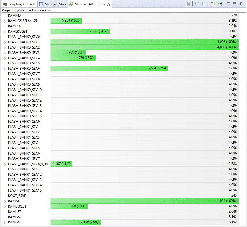
The memory allocation is shown in Figure 3-8
 Figure 3-8 TIDM-02008 Memory
Allocation