TIDUD61E October   2020  – April 2021


  1.   Description
  2.   Resources
  3.   Features
  4.   Applications
  5.   5
  6. 1System Description
    1. 1.1 Key System Specifications
  7. 2System Overview
    1. 2.1 Block Diagram
    2. 2.2 Design Considerations
      1. 2.2.1 Input AC Voltage Sensing
      2. 2.2.2 Bus Voltage Sensing
      3. 2.2.3 AC Current Sensing
      4. 2.2.4 Sense Filter
      5. 2.2.5 Protection (CMPSS)
    3. 2.3 Highlighted Products
      1. 2.3.1 C2000™ MCU F28004x
      2. 2.3.2 LMG3410R070
      3. 2.3.3 UCC27714
    4. 2.4 System Design Theory
      1. 2.4.1 PWM
      2. 2.4.2 Current Loop Model (PFC and Inverter mode)
      3. 2.4.3 DC Bus Regulation Loop (for PFC mode only)
      4. 2.4.4 Soft Start Around Zero Crossing for Eliminate or Reduce Current Spike
      5. 2.4.5 AC Drop Test
  8. 3Hardware, Software, Testing Requirements, and Test Results
    1. 3.1 Required Hardware and Software
      1. 3.1.1 Hardware
        1. 3.1.1.1 Base Board Settings
        2. 3.1.1.2 Control Card Settings
      2. 3.1.2 Software
        1. 3.1.2.1 Opening Project Inside CCS
        2. 3.1.2.2 Project Structure
        3. 3.1.2.3 Using CLA on C2000 MCU to Alleviate CPU Burden
        4. 3.1.2.4 CPU and CLA Utilization and Memory Allocation
        5. 3.1.2.5 Running the Project
          1. 3.1.2.5.1 Lab 1: Open Loop, DC (PFC Mode)
            1. 3.1.2.5.1.1 Setting Software Options for LAB 1
            2. 3.1.2.5.1.2 Building and Loading Project
            3. 3.1.2.5.1.3 Setup Debug Environment Windows
            4. 3.1.2.5.1.4 Using Real-Time Emulation
            5. 3.1.2.5.1.5 Running Code
          2. 3.1.2.5.2 Lab 2: Closed Current Loop DC (PFC)
            1. 3.1.2.5.2.1 Setting Software Options for Lab 2
            2. 3.1.2.5.2.2 Designing Current Loop Compensator
            3. 3.1.2.5.2.3 Building and Loading Project and Setting up Debug
            4. 3.1.2.5.2.4 Running Code
          3. 3.1.2.5.3 Lab 3: Closed Current Loop, AC (PFC)
            1. 3.1.2.5.3.1 Setting Software Options for Lab 3
            2. 3.1.2.5.3.2 Building and Loading Project and Setting up Debug
            3. 3.1.2.5.3.3 Running Code
          4. 3.1.2.5.4 Lab 4: Closed Voltage and Current Loop (PFC)
            1. 3.1.2.5.4.1 Setting Software Options for Lab 4
            2. 3.1.2.5.4.2 Designing Voltage Loop Compensator
            3. 3.1.2.5.4.3 Building and Loading Project and Setting up Debug
            4. 3.1.2.5.4.4 Running Code
          5. 3.1.2.5.5 Lab 5: Open loop, DC (Inverter)
            1. 3.1.2.5.5.1 Setting Software Options for Lab 5
            2. 3.1.2.5.5.2 Building and Loading Project
            3. 3.1.2.5.5.3 Setup Debug Environment Windows
            4. 3.1.2.5.5.4 Running Code
          6. 3.1.2.5.6 Lab 6: Open loop, AC (Inverter)
            1. 3.1.2.5.6.1 Setting Software Options for Lab 6
            2. 3.1.2.5.6.2 Building and Loading Project and Setting up Debug
            3. 3.1.2.5.6.3 Running Code
          7. 3.1.2.5.7 Lab 7: Closed Current Loop, DC (Inverter with resistive load)
            1. 3.1.2.5.7.1 Setting Software Options for Lab 7
            2. 3.1.2.5.7.2 Designing Current Loop Compensator
            3. 3.1.2.5.7.3 Building and Loading Project and Setting up Debug
            4. 3.1.2.5.7.4 Running Code
          8. 3.1.2.5.8 Lab 8: Closed Current Loop, AC (Inverter with resistive load)
            1. 3.1.2.5.8.1 Setting Software Options for Lab 8
            2. 3.1.2.5.8.2 Building and Loading Project and Setting up Debug
            3. 3.1.2.5.8.3 Running Code
          9. 3.1.2.5.9 Lab 9: Closed Current Loop (Grid Connected Inverter)
            1. 3.1.2.5.9.1 Setting Software Options for Lab 9
            2. 3.1.2.5.9.2 Building and Loading Project and Setting up Debug
            3. 3.1.2.5.9.3 Running Code: Emulated Grid-tied Condition (Verification purpose only)
            4. 3.1.2.5.9.4 Running Code: Grid-tied Condition
        6. 3.1.2.6 Running Code on CLA
        7. 3.1.2.7 Advanced Options
          1. 3.1.2.7.1 Input Cap Compensation for PF Improvement Under Light Load
          2. 3.1.2.7.2 83
          3. 3.1.2.7.3 Adaptive Dead Time for Efficiency Improvements
          4. 3.1.2.7.4 Phase Shedding for Efficiency Improvements
          5. 3.1.2.7.5 Non-Linear Voltage Loop for Transient Reduction
          6. 3.1.2.7.6 Software Phase Locked Loop Methods: SOGI - FLL
    2. 3.2 Testing and Results
      1. 3.2.1 Test Results at Input 120 Vrms, 60 Hz, Output 380-V DC
        1. 3.2.1.1 Startup
        2. 3.2.1.2 Steady State Condition
        3. 3.2.1.3 Transient Test With Step Load Change
          1. 3.2.1.3.1 0% to 50% Load Step Change
          2. 3.2.1.3.2 50% to 100% Load Step Change
          3. 3.2.1.3.3 100% to 50% Load Step Change
          4. 3.2.1.3.4 50% to 100% Load Step Change
      2. 3.2.2 Test Results at Input 230 Vrms, 50 Hz, Output 380 V DC
        1. 3.2.2.1 Startup
        2. 3.2.2.2 Steady State Condition
        3. 3.2.2.3 Transient Test With Step Load Change
          1. 3.2.2.3.1 33% to 100% Load Step Change
          2. 3.2.2.3.2 100% to 33% Load Step Change
      3. 3.2.3 Test Results Graphs
  9. 4Design Files
    1. 4.1 Schematics
    2. 4.2 Bill of Materials
    3. 4.3 PCB Layout Recommendations
      1. 4.3.1 Layout Prints
    4. 4.4 Altium Project
    5. 4.5 Gerber Files
    6. 4.6 Assembly Drawings
  10. 5Software Files
  11. 6Related Documentation
    1. 6.1 Trademarks
  12. 7About the Author
  13. 8Revision History
Adaptive Dead Time for Efficiency Improvements

In continuous conduction mode, the dead-time control for synchronous rectification is critical in terms of short-circuit protection and efficiency. With the optimal dead time, the risk of shoot through can be eliminated and it also prevents an excessive conduction loss from body diode conduction of Sync FET. Therefore, the goal of optimal dead time is not to turn on the Active FET and Sync FET simultaneously while minimize a redundant third quadrant conduction of Sync FET.

This optimal dead time can be calculated from the measured current and the device output capacitance, this is given by Equation 11.

Equation 11. GUID-E607667C-B0F3-4927-AF4C-B3A402399563-low.gif

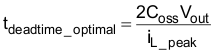
Figure 3-48 shows the block diagram for implementation.

GUID-BF93DD49-D65C-44B1-A1A6-BE46F9B0382A-low.gifFigure 3-48 Adaptive Dead-Time Implementation

The option enables power saving, which is shown for the high line case in Figure 3-49 compared to a fixed dead time from which it can be inferred that avoiding the shoot through at low power levels results in significant power savings. However, once the shoot through is avoided the power savings drop first and then progressively increase as power increases and the diode conduction time is reduced by implementing adaptive dead-time adjustment.

GUID-0BD482FB-F4ED-4393-9E0F-6D74CA8CD2FE-low.gifFigure 3-49 Power Savings With Adaptive Dead-Time at High Line 230 Vrms

To enable adaptive dead time, select the drop down box under Project Options on the powerSUITE page of the solution. For FED the fixed value that is specified on the main.syscfg is used. When adaptive dead time is enabled the RED is modulated and the minimum and maximum bounds are specified in the <solution>_user_settings.h. The following are the #define that can be adjusted:

#define TTPLPFC_HF_FET_COSS  (float32_t) 0.000000000145 
#define TTPLPFC_PFC_DEADBAND_RED_MIN_US (float32_t) 0.020  
#define TTPLPFC_PFC_DEADBAND_RED_MAX_US (float32_t) 0.200 
            

Following these adjustments the project must be saved, re-compiled, and loaded on the controller when this option is changed. Hardware setup and software instructions as outlined in Section 3.1.2.5.4 can be followed to see the behavior of the board and measure efficiency.