TIDUD61E October 2020 – April 2021
- Description
- Resources
- Features
- Applications
- 5
- 1System Description
- 2System Overview
-
3Hardware, Software, Testing Requirements, and Test Results
- 3.1
Required Hardware and Software
- 3.1.1 Hardware
- 3.1.2
Software
- 3.1.2.1 Opening Project Inside CCS
- 3.1.2.2 Project Structure
- 3.1.2.3 Using CLA on C2000 MCU to Alleviate CPU Burden
- 3.1.2.4 CPU and CLA Utilization and Memory Allocation
- 3.1.2.5
Running the Project
- 3.1.2.5.1 Lab 1: Open Loop, DC (PFC Mode)
- 3.1.2.5.2 Lab 2: Closed Current Loop DC (PFC)
- 3.1.2.5.3 Lab 3: Closed Current Loop, AC (PFC)
- 3.1.2.5.4 Lab 4: Closed Voltage and Current Loop (PFC)
- 3.1.2.5.5 Lab 5: Open loop, DC (Inverter)
- 3.1.2.5.6 Lab 6: Open loop, AC (Inverter)
- 3.1.2.5.7 Lab 7: Closed Current Loop, DC (Inverter with resistive load)
- 3.1.2.5.8 Lab 8: Closed Current Loop, AC (Inverter with resistive load)
- 3.1.2.5.9 Lab 9: Closed Current Loop (Grid Connected Inverter)
- 3.1.2.6 Running Code on CLA
- 3.1.2.7
Advanced Options
- 3.1.2.7.1 Input Cap Compensation for PF Improvement Under Light Load
- 3.1.2.7.2 83
- 3.1.2.7.3 Adaptive Dead Time for Efficiency Improvements
- 3.1.2.7.4 Phase Shedding for Efficiency Improvements
- 3.1.2.7.5 Non-Linear Voltage Loop for Transient Reduction
- 3.1.2.7.6 Software Phase Locked Loop Methods: SOGI - FLL
- 3.2 Testing and Results
- 3.1
Required Hardware and Software
- 4Design Files
- 5Software Files
- 6Related Documentation
- 7About the Author
- 8Revision History
3.1.2.5.2.4 Running Code
- The project is programmed to drive the inrush relay and clear the trip after a set amount of time, that is, autoStartSlew==100. The software is programmed to do so in this lab. An input voltage must be applied after hitting run and before this autoslew counter reaches 100. If the counter reaches 100, before voltage is applied at the input, the code must be reset. For which the controller must be brought out of real time mode, a reset performed and restarted. Repeat steps from 3
- Now run the project by clicking
 .
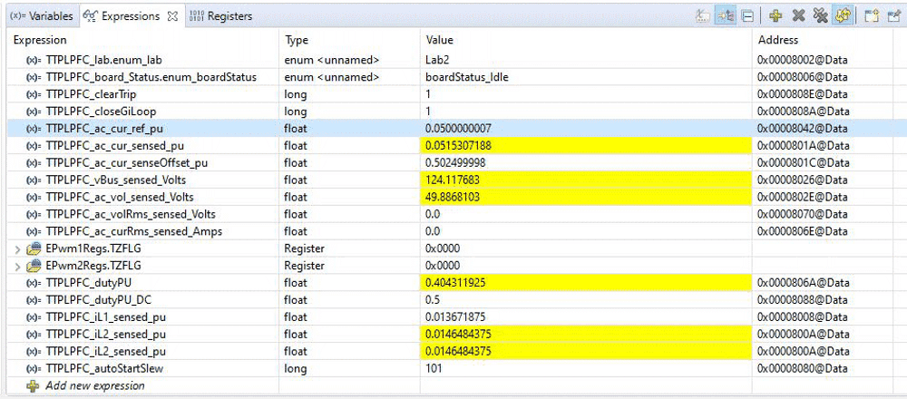
. - Apply an input voltage of approximately 50 V before the TTPLPFC_autoStartSlew reaches 100. As soon TTPLPFC_autoStartSlew reaches 100, the inrush relay is triggered, and PWM trip is cleared along with closing the current loop flag.
 Figure 3-16 Watch Expression, Lab 2, After Closed Current Loop Operation Begins
 - The input current regulates around 0.7 A, and the output voltage boosts to approximately 128 V.
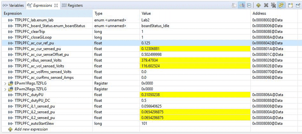
- Now slowly increase TTPLPFC_ac_cur_ref_pu to 0.1, that is, 2.5-A input.
- Next slowly increase Vin = 120 V, and the output voltage will be greater than 350 V.
 Figure 3-17 Watch Expression, Lab 2, After Closed Current Loop Operation Begins at Full Voltage
 - SFRA is integrated in the software of this build to verify the designed compensator provides enough gain and phase margin by measuring on hardware. To run the SFRA keep the project running, and from the cfg page, click on the SFRA icon. SFRA GUI appears.
- Select the options for the device on the SFRA GUI. For example, for F28004x select floating point. Click on Setup Connection. On the pop-up window uncheck the boot on connect option, and select an appropriate COM port. Ensure Boot on Connect is deselected. Click OK. Return to the SFRA GUI, and click Connect.
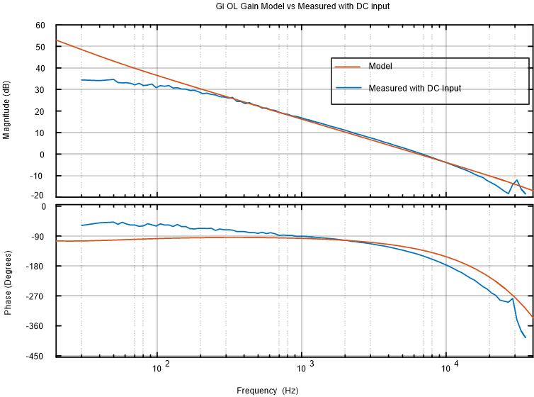
- The SFRA GUI connects to the device. A SFRA sweep can now be started by clicking Start Sweep. The complete SFRA sweep takes a few minutes to finish. Activity can be monitored by seeing the progress bar on the SFRA GUI and also checking the flashing of blue LED on the back on the control card that indicates UART activity. Once complete, a graph with the open loop plot appears. Comparing this with the measured plots, there is good correlation between the modeled and measured as shown in Figure 3-18. This verifies that the designed compensator is indeed stable and the model accurate. Note: the deviation at low frequency, less than 200 Hz, is expected and is a known phenomena, also the measurement shown here was taken with a DC source, if an AC source is used to emulate a DC source the output impedance of the AC source can result in deviations from the graph plotted below
 Figure 3-18 SFRA Run vs Modeled Closed Current Loop, Open Loop Gain
The frequency response data is also saved in the project folder under an SFRA data folder and is time stamped with the time of the SFRA run.
- Optionally one can use the measured frequency response of the plant to design the current compensator by clicking on the Compensation Designer again from the syscfg page and choose SFRA Data for plant option on the GUI. This uses the measured plant information to design the compensator. This option can be used to fine tune the compensation. By default the compensation designer points to the latest SFRA run. If a previous SFRA run plant information must be used the user can select the SFRAData.csv file by browsing to it by clicking on Browse SFRA Data.
- This action verifies the current compensator design.
- To bring the system to a safe stop, bring the input DC voltage down to zero, observe the TTPLPFC_vBus_sensed_Volts comes down to zero as well.
- Fully halting the MCU when in real-time mode is a two-step process. First halt the processor by using the Halt button on the toolbar (
 ) or by using Target → Halt. Then take the MCU out of real-time mode by clicking on
  . Finally, reset the MCU (
 ) .
) . - Close the CCS debug session by clicking Terminate Debug Session (Target → Terminate all).
