TIDUD61E October 2020 – April 2021
- Description
- Resources
- Features
- Applications
- 5
- 1System Description
- 2System Overview
-
3Hardware, Software, Testing Requirements, and Test Results
- 3.1
Required Hardware and Software
- 3.1.1 Hardware
- 3.1.2
Software
- 3.1.2.1 Opening Project Inside CCS
- 3.1.2.2 Project Structure
- 3.1.2.3 Using CLA on C2000 MCU to Alleviate CPU Burden
- 3.1.2.4 CPU and CLA Utilization and Memory Allocation
- 3.1.2.5
Running the Project
- 3.1.2.5.1 Lab 1: Open Loop, DC (PFC Mode)
- 3.1.2.5.2 Lab 2: Closed Current Loop DC (PFC)
- 3.1.2.5.3 Lab 3: Closed Current Loop, AC (PFC)
- 3.1.2.5.4 Lab 4: Closed Voltage and Current Loop (PFC)
- 3.1.2.5.5 Lab 5: Open loop, DC (Inverter)
- 3.1.2.5.6 Lab 6: Open loop, AC (Inverter)
- 3.1.2.5.7 Lab 7: Closed Current Loop, DC (Inverter with resistive load)
- 3.1.2.5.8 Lab 8: Closed Current Loop, AC (Inverter with resistive load)
- 3.1.2.5.9 Lab 9: Closed Current Loop (Grid Connected Inverter)
- 3.1.2.6 Running Code on CLA
- 3.1.2.7
Advanced Options
- 3.1.2.7.1 Input Cap Compensation for PF Improvement Under Light Load
- 3.1.2.7.2 83
- 3.1.2.7.3 Adaptive Dead Time for Efficiency Improvements
- 3.1.2.7.4 Phase Shedding for Efficiency Improvements
- 3.1.2.7.5 Non-Linear Voltage Loop for Transient Reduction
- 3.1.2.7.6 Software Phase Locked Loop Methods: SOGI - FLL
- 3.2 Testing and Results
- 3.1
Required Hardware and Software
- 4Design Files
- 5Software Files
- 6Related Documentation
- 7About the Author
- 8Revision History
2.4.2 Current Loop Model (PFC and Inverter mode)
The same control loop model applies to both PFC and grid-tied inverter operation. To understand the current loop model, first look at the inductor current closely. In Figure 2-8 the Duty cycle (D) is provided to the PWM modulator, which is connected to the switch Q3 and Q4. From here, Equation 1 is written as:
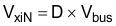
When D is set to 1, Q3 is on all the time, and when D is 0, Q3 is off all the time.
To modulate the current through the inductor, the voltage  is regulated using the duty cycle control of Q3 and Q4 switches. It is assumed that the direction of current is positive in the direction from the AC line into the rectifier and that the grid is fairly stiff when using the DC bus feedforward and the AC voltage feedforward. Figure 2-9 shows the simplified current loop, and the current loop plant model is written as Equation 2.
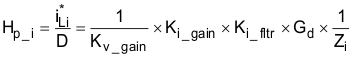
Where:
- Kv_gain is the inverse of maximum bus voltage sensed,
- Kvac_gain is the inverse of maximum AC voltage sensed, (A factor to normalize this is applied in the feedforward and hence the current loop model is only dependent on the Kv_gain)
 is the inverse of maximum AC current sensed,
 is the response of the RC filter connected from the current sensor to the ADC pin
 is the digital delay associated with the PWM update and digital control is the current command
 is the current command
 Figure 2-9
Current Loop Control Model
Figure 2-9
Current Loop Control ModelThe negative sign on the reference is because the current loop is thought to be regulating the voltage, . To increase the current, must be reduced—hence, the opposite sign for reference and feedback in Figure 2-9.
This current loop model is then used to design the current compensator. A simple proportional integral controller is used for the current loop.
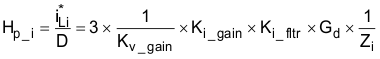
Now, in the case of three interleaved phases, the current is simply three times more as the same duty cycle is provided to each leg. Hence, the plant model is given as Equation 3.
This model is verified on this design using the SFRA library. Figure 2-10 shows the model versus measured open loop frequency response, which shows good correlation between the two.
 Figure 2-10 Gi, Current Open Loop Gain Measured Verus Modelled