TIDUDJ6B August   2022  – February 2023 OPA388-Q1


  1.   Description
  2.   Resources
  3.   Features
  4.   Applications
  5.   5
  6. 1System Description
    1. 1.1 Key System Specifications
  7. 2System Overview
    1. 2.1 Block Diagrams
    2. 2.2 Highlighted Products
      1. 2.2.1 TPSI2140-Q1
      2. 2.2.2 AMC1301-Q1
      3. 2.2.3 SN6501-Q1
    3. 2.3 System Design Theory
      1. 2.3.1 Isolation Leakage Current Theory
      2. 2.3.2 High-Voltage Measurement
  8. 3Hardware, Testing Requirements, and Test Results
    1. 3.1 Required Hardware
    2.     Hardware with Solid-State Relay
    3. 3.2 Testing and Results
      1. 3.2.1 Test Setup
      2. 3.2.2 Isolation Tests
        1. 3.2.2.1 Normal Conditions
        2. 3.2.2.2 Isolation Error at HV Positive
        3. 3.2.2.3 Isolation Error at HV Negative
        4. 3.2.2.4 Isolation Error at ¼ HV Battery Voltage
        5. 3.2.2.5 Isolation Error at ¾ HV Battery Voltage
        6. 3.2.2.6 Isolation Error at the Middle of an HV Battery Voltage
      3. 3.2.3 Solid-State Relay Isolation Tests
        1. 3.2.3.1 Normal Conditions
        2. 3.2.3.2 Isolation Error at HV Positive
        3. 3.2.3.3 Isolation Error at HV Negative
        4. 3.2.3.4 Isolation Error at ¼ HV Battery Voltage
        5. 3.2.3.5 Isolation Error at ¾ HV Battery Voltage
        6. 3.2.3.6 Isolation Error at the Middle of an HV Battery Voltage
      4. 3.2.4 High Voltage Measurements
      5. 3.2.5 Isolation Measurement Analysis
      6. 3.2.6 Error Analysis
  9. 4Design Files
    1. 4.1 Schematics
    2. 4.2 Bill of Materials
    3. 4.3 PCB Layout Recommendations
      1. 4.3.1 Layout Prints
    4. 4.4 Altium Project
    5. 4.5 Gerber Files
    6. 4.6 Assembly Drawings
  10. 5Software Files
  11. 6Related Documentation
  12. 7Trademarks
  13. 8Revision History

PCB Layout Recommendations

The PCB layout for isolation leakage current measurements must be based on the requirements and components selected for the design.

  • The high-voltage section of the system must not have any polygons to HV positive, HV negative, or chassis ground.
  • Place MELF resistors in series or a series parallel combination that maintains the isolation and does not allow any low-ohmic paths due to PCB, humidity, or liquids, which are all probable occurrences on the PCB.
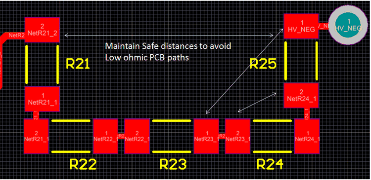
    GUID-5507BEE8-7DE9-4B64-9A23-DE18B8F62F5F-low.gifFigure 4-1 Placing MELF Resistors
  • Maintain creepage and clearance distances required for isolation components (AMC1301-Q1) as explained in the device data sheet.
  • To minimize noise, take care when placing analog lines to avoid noise from relays and power switching components.
  • Follow the component data sheet to minimize the EMC issues on layout.