TIDUEO0C July 2019 – March 2021
- Description
- Resources
- Features
- Applications
- 5
- 1System Description
-
2System Overview
- 2.1 Block Diagram
- 2.2 Design Considerations
- 2.3
Highlighted Products
- 2.3.1 TPS63900: 1.8V-5.5 VIN Buck-Boost Converter With 75-nA Ultra-low Quiescent Current and 400-mA Output Current
- 2.3.2 TPS610995: 0.7 VIN Synchronous Boost Converter With 400-nA Ultra-low Quiescent Current and 1-A Peak Current
- 2.3.3 TPS62840: 750-mA Synchronous Step-Down Converter With Ultra-low Quiescent Current Consumption
- 2.4 System Design Theory
- 3Hardware, Software, Testing Requirements, and Test Results
- 4Design Files
- 5Software Files
- 6Related Documentation
- 7Terminology
- 8About the Author
- 9Revision History
3.2.2.3 Test Results With the TPS63900 Buck-Boost Converter NB
 Figure 3-11 TPS63900 Buck-Boost Battery Discharge Graph (1s1p
Configuration)
 Figure 3-12 TPS63900 Buck-Boost Battery Discharge Graph (1s2p
Configuration)
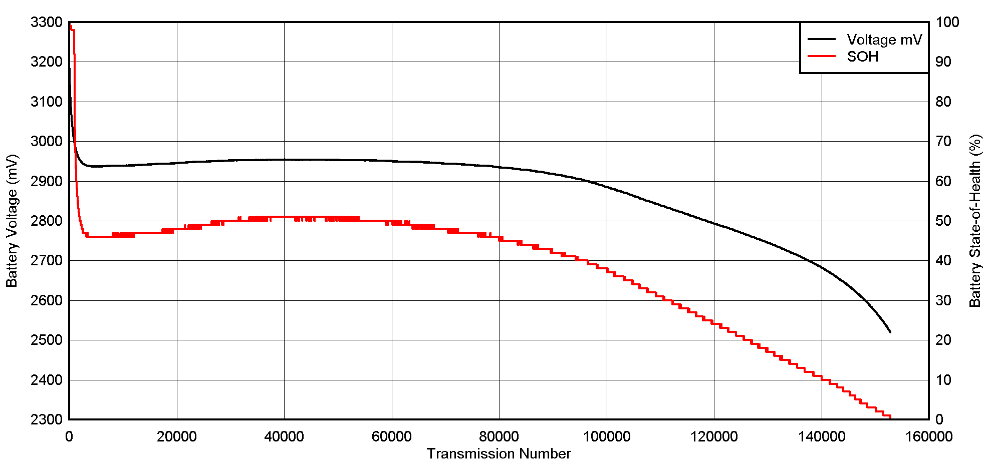
Figure 3-12 TPS63900 Buck-Boost Battery Discharge Graph (1s2p
Configuration)Figure 3-11 and Figure 3-12 demonstrate that when using this power solution, the system supports approximately 75,000 transmission cycles for the 1s1p and 141,000 transmission cycles for the 1s2p (taken at from 100% to 10% SOH) for the simulated NB-IoT load profile. The advantages of using the TPS63900 Buck-Boost Converter is not only its low quiescent current consumption (75 nA typical), but also its high efficiency at light load that minimizes the power losses during the non-transmission period. All of this results in extended product lifetime.
Another feature of the TPS63900 that makes it useful for NB-IoT applications is the dynamic voltage scaling. The part can provide two output voltage levels using two external resistor dividers and by controlling the select pin. This can be used to provide a higher voltage during NB-IoT transmission cycles and can be switched to provide the lower voltage during normal operation when no transmissions are occurring. This feature can be used to further extend the number of transmission cycles shown above.