TIDUEY6 April 2021
- Description
- Resources
- Features
- Applications
- 5
- 1System Description
- 2System Overview
-
3Hardware, Software, Testing Requirements, and Test Results
- 3.1
Hardware Requirements
- 3.1.1
Hardware Overview
- 3.1.1.1
Control Module
- 3.1.1.1.1
Control Mother Board
- 3.1.1.1.1.1 Inverter Safing - UCC5870 ASC and Fault Control
- 3.1.1.1.1.2 DC-DC Safing
- 3.1.1.1.1.3 DC-DC Converter Secondary PWM Selection
- 3.1.1.1.1.4 Blower Fan Control
- 3.1.1.1.1.5 Voltage Monitor
- 3.1.1.1.1.6 Resolver Interface Control
- 3.1.1.1.1.7 Test Points on Control Module
- 3.1.1.1.1.8 General Purpose Ports
- 3.1.1.1.1.9 Connectors and Headers on Control Mother Board
- 3.1.1.1.2 Power Supplies
- 3.1.1.1.3 TCAN4550 module
- 3.1.1.1.4 Dual TCAN Module
- 3.1.1.1.5 Analog Back End Module
- 3.1.1.1.6 Resolver Analog Front End Module
- 3.1.1.1.1
Control Mother Board
- 3.1.1.2 Inverter Module
- 3.1.1.3 DC-DC Bidirectional Converter Module
- 3.1.1.1
Control Module
- 3.1.1
Hardware Overview
- 3.2 Resource Mapping
- 3.3 Test Setup
- 3.4 Test Results
- 3.1
Hardware Requirements
- 4General Texas Instruments High Voltage Evaluation (TI HV EVM) User Safety Guidelines
- 5Design and Documentation Support
- 6About the Author
3.1.1.2.4 Inverter Voltage Sense Module
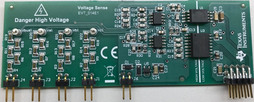
Voltage sense module is designed to provide digital feedback of inverter phase output voltages and analog feedback of DC bus voltage. All feedback signals are isolated. Digital feedback is provided by ISO7240CF-Q1 and some standard linear parts. Analog differential feedback is provided by TI's isolation amplifier AMC1311-Q1 and is based on ±480-V isolated voltage-sensing circuit with differential output. A picture of this board is shown in Figure 3-25.
 Figure 3-25 Inverter
Voltage Sense Board
Figure 3-25 Inverter
Voltage Sense BoardAMC1311 provides a good linear performance for an input voltage range of 2 V with high source impedance. It has low offset error and drift, fixed gain of 1 with very low gain error and drift and low non-linearity and drift, and has an output bandwidth of above 200 KHz. For DC measurement, this is substantially superior.
AMC1311 requires separate power supplies for the high voltage (HOT) and low voltage (COLD) sides. Isolated power supply for the HOT side of AMC1311 is derived from one of the low side gate drive's secondary power supply (CL) and drop regulated to 3.3 V. COLD side power supply is fed in through a 4x2 connector. This module is mounted on headers J20, J23, J24, J25, J26 and J27 of the inverter mother board. Feedback signals are brought out to 4x2 connector J20 of the inverter mother board.