TIDUEY6 April 2021
- Description
- Resources
- Features
- Applications
- 5
- 1System Description
- 2System Overview
-
3Hardware, Software, Testing Requirements, and Test Results
- 3.1
Hardware Requirements
- 3.1.1
Hardware Overview
- 3.1.1.1
Control Module
- 3.1.1.1.1
Control Mother Board
- 3.1.1.1.1.1 Inverter Safing - UCC5870 ASC and Fault Control
- 3.1.1.1.1.2 DC-DC Safing
- 3.1.1.1.1.3 DC-DC Converter Secondary PWM Selection
- 3.1.1.1.1.4 Blower Fan Control
- 3.1.1.1.1.5 Voltage Monitor
- 3.1.1.1.1.6 Resolver Interface Control
- 3.1.1.1.1.7 Test Points on Control Module
- 3.1.1.1.1.8 General Purpose Ports
- 3.1.1.1.1.9 Connectors and Headers on Control Mother Board
- 3.1.1.1.2 Power Supplies
- 3.1.1.1.3 TCAN4550 module
- 3.1.1.1.4 Dual TCAN Module
- 3.1.1.1.5 Analog Back End Module
- 3.1.1.1.6 Resolver Analog Front End Module
- 3.1.1.1.1
Control Mother Board
- 3.1.1.2 Inverter Module
- 3.1.1.3 DC-DC Bidirectional Converter Module
- 3.1.1.1
Control Module
- 3.1.1
Hardware Overview
- 3.2 Resource Mapping
- 3.3 Test Setup
- 3.4 Test Results
- 3.1
Hardware Requirements
- 4General Texas Instruments High Voltage Evaluation (TI HV EVM) User Safety Guidelines
- 5Design and Documentation Support
- 6About the Author
3.1.1.3.2 DC-DC Gate Driver Module
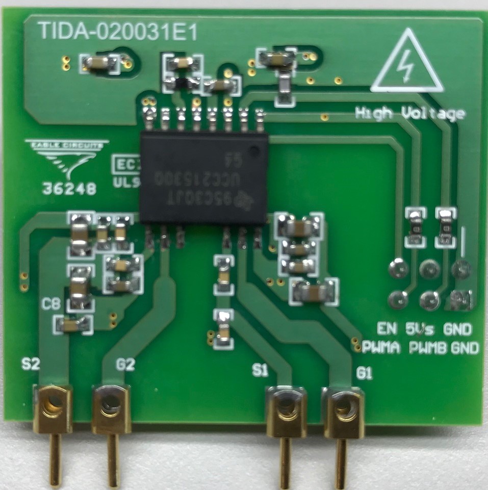
Isolated gate drive module for DC-DC is designed as a separate daughter card to drive a high voltage half-bridge. This is to reduce contact lengths between power supplies and gate driver secondary circuits and reduce routing complexity. This module is designed using UCC21530-Q1 isolated half bridge gate driver and SN6505-Q1 isolated power supply driver. The UCC21530 supports enable function which allows the MCU to disable power stage independent of PWM output. The isolated power supply is designed with a second layer of enable and designed to generate gate drive voltages of +15 V and -4 V for the SiC MOSFET selected for the primary full bridge. The power supply is designed based on a regulated 5 V input with no secondary regulation. A picture of the board is shown in Figure 3-28.
 Figure 3-28 DC-DC Isolated Gate
Driver