Packaging information
| Package | Pins BGA (NXA) | 292 |
| Operating temperature range (°C) -40 to 85 |
| Package qty | Carrier 40 | JEDEC TRAY (10+1) |
Features for the ADC12D1800
- Configurable to Either 3.6 GSPS Interleaved or 1.8 GSPS Dual ADC
- Pin-Compatible with ADC10D1000/1500 and ADC12D1000/1600
- Internally Terminated, Buffered, Differential Analog Inputs
- Interleaved Timing Automatic and Manual Skew Adjust
- Test Patterns at Output for System Debug
- Programmable 15-bit Gain and 12-bit Plus Sign Offset
- Programmable tAD Adjust Feature
- 1:1 Non-Demuxed or 1:2 Demuxed LVDS Outputs
- AutoSync Feature for Multi-Chip Systems
- Single 1.9-V ± 0.1-V Power Supply
- Key
Specifications
- Resolution: 12 Bits
- Interleaved 3.6 GSPS
ADC
- Noise Floor Density –153.5 dBm/Hz (typ)
- IMD3 –61 dBFS (typ)
- Noise Power Ratio 48.5 dB (typ)
- Power 4.4 W (typ)
- Full Power Bandwidth 1.75 GHz (typ)
- Dual 1.8 GSPS ADC, Fin =
125MHz
- ENOB: 9.4 (typ)
- SNR 58.5 dB (typ)
- SFDR 73 dBc (typ)
- Power 4.4 W (typ)
- Full Power Bandwidth 2.8 GHz (typ)
Description for the ADC12D1800
The 12-bit, 3.6 GSPS ADC12D1800 is the latest advance in TI’s Ultra-High-Speed ADC family and builds upon the features, architecture and functionality of the 10-bit GHz family of ADCs.
The ADC12D1800 provides a flexible LVDS interface which has multiple SPI programmable options to facilitate board design and FPGA/ASIC data capture. The LVDS outputs are compatible with IEEE 1596.3-1996 and supports programmable common mode voltage.
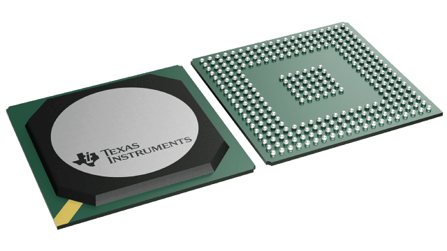
The product is packaged in a leaded or lead-free 292-ball thermally enhanced BGA package over the rated industrial temperature range of –40°C to +85°C.
To achieve full rated performance for fCLK > 1.6 GHz, write the maximum power settings one time to Register 6h through the serial interface; see Section 5.6.1 for more information.