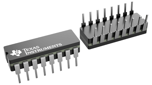
Packaging information
| Package | Pins CDIP (J) | 16 |
| Operating temperature range (°C) -55 to 125 |
| Package qty | Carrier 25 | TUBE |
Features for the SN54LS139A
- Designed Specifically for High-Speed:
- Memory Decoders
- Data Transmission Systems
- Two Fully Independent 2- to 4-Line
Decoders/Demultiplexers - Schottky clamped for High Performance
Description for the SN54LS139A
These Schottky-clamped TTL MSI circuits are designed to be used in high-performance memory-decoding or data-routing applications requiring very short propagation delay times. In high-performance memory systems, these decoders can be used to minimize the effects of system decoding. When employed with high-speed memories utilizing a fast-enable circuit, the delay times of these decoders and the enable time of the memory are usually less than the typical access time of the memory. This means that the effective system delay introduced by the Schottky-clamped system decoder is negligible.
The circuit comprises two individual two-line to four-line decoders in a single package. The active-low enable input can be used as a data line in demultiplexing applications.
All of these decoders/demultiplexers feature fully buffered inputs, each of which represents only one normalized load to its driving circuit. All inputs are clamped with high-performance Schottky diodes to suppress line-ringing and to simplify system design. The SN54LS139A and SN54S139 are characterized for operation range of –55°C to 125°C. The SN74LS139A and SN74S139A are characterized for operation from 0°C to 70°C.
