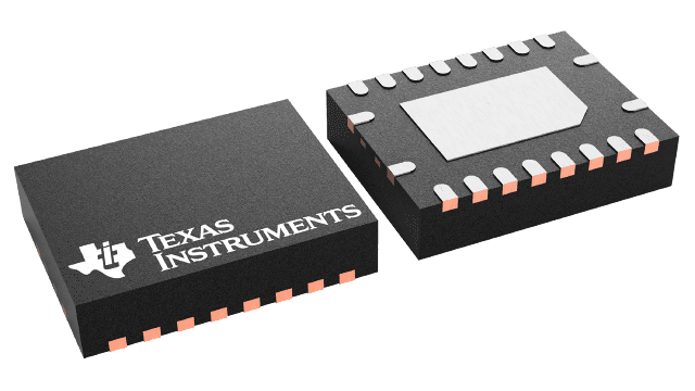
Packaging information
| Package | Pins VQFN (RGY) | 20 |
| Operating temperature range (°C) -40 to 85 |
| Package qty | Carrier 3,000 | LARGE T&R |
Features for the SN74AUCH245
- Optimized for 1.8-V Operation and Is 3.6-V I/O Tolerant to Support Mixed-Mode Signal Operation
- Ioff Supports Partial-Power-Down Mode Operation
- Sub 1-V Operable
- Max tpd of 2 ns at 1.8 V
- Low Power Consumption, 20-µA Max ICC
- ±8-mA Output Drive at 1.8 V
- Bus Hold on Data Inputs Eliminates the Need for External Pullup/Pulldown Resistors
- Latch-Up Performance Exceeds 100 mA Per JESD 78, Class II
- ESD Protection Exceeds JESD 22
- 2000-V Human-Body Model (A114-A)
- 200-V Machine Model (A115-A)
- 1000-V Charged-Device Model (C101)
Description for the SN74AUCH245
This octal bus transceiver is operational at 0.8-V to 2.7-V VCC, but is designed specifically for 1.65-V to 1.95-V VCC operation.
The SN74AUCH245 is designed for asynchronous communication between data buses. The device transmits data from the A bus to the B bus or from the B bus to the A bus, depending on the logic level at the direction-control (DIR) input. The output-enable (OE)\ input can be used to disable the device so the buses are effectively isolated.
To ensure the high-impedance state during power up or power down, OE\ should be tied to VCC through a pullup resistor; the minimum value of the resistor is determined by the current-sinking capability of the driver.
Active bus-hold circuitry holds unused or undriven inputs at a valid logic state. Use of pullup or pulldown resistors with the bus-hold circuitry is not recommended.
This device is fully specified for partial-power-down applications using Ioff. The Ioff circuitry disables the outputs, preventing damaging current backflow through the device when it is powered down.