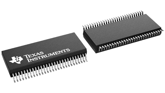
Packaging information
| Package | Pins SSOP (DL) | 56 |
| Operating temperature range (°C) -40 to 85 |
| Package qty | Carrier 20 | TUBE |
Features for the SN74LVTH16652
- Members of the Texas Instruments WidebusTM Family
- State-of-the-Art Advanced BiCMOS Technology (ABT) Design for 3.3-V Operation and Low Static-Power Dissipation
- Support Mixed-Mode Signal Operation (5-V Input and Output Voltages With 3.3-V VCC)
- Support Unregulated Battery Operation Down to 2.7 V
- Typical VOLP (Output Ground Bounce) < 0.8 V at VCC = 3.3 V, TA = 25°C
- Ioff and Power-Up 3-State Support Hot Insertion
- Bus Hold on Data Inputs Eliminates the Need for External Pullup/Pulldown Resistors
- Distributed VCC and GND Pin Configuration Minimizes High-Speed Switching Noise
- Flow-Through Architecture Optimizes PCB Layout
- Latch-Up Performance Exceeds 500 mA Per JESD 17
- ESD Protection Exceeds 2000 V Per MIL-STD-883, Method 3015; Exceeds 200 V Using Machine Model (C = 200 pF, R = 0)
- Package Options Include Plastic Shrink Small-Outline (DL) and Thin Shrink Small-Outline (DGG) Packages and 380-mil Fine-Pitch Ceramic Flat (WD) Package Using 25-mil Center-to-Center Spacings
Widebus is a trademark of Texas Instruments Incorporated.
Description for the SN74LVTH16652
The 'LVTH16652 devices are 16-bit bus transceivers designed for low-voltage (3.3-V) VCC operation, but with the capability to provide a TTL interface to a 5-V system environment. These devices can be used as two 8-bit transceivers or one 16-bit transceiver.
Output-enable (OEAB and OEBA\) inputs are provided to control the transceiver functions. Select-control (SAB and SBA) inputs are provided to select whether real-time or stored data is transferred. A low input level selects real-time data, and a high input level selects stored data. The circuitry used for select control eliminates the typical decoding glitch that occurs in a multiplexer during the transition between stored and real-time data. Figure 1 illustrates the four fundamental bus-management functions that can be performed with the 'LVTH16652 devices.
Data on the A or B bus, or both, can be stored in the internal D flip-flops by low-to-high transitions at the appropriate clock (CLKAB or CLKBA) inputs, regardless of the levels on the select-control or output-enable inputs. When SAB and SBA are in the real-time transfer mode, it also is possible to store data without using the internal D-type flip-flops by simultaneously enabling OEAB and OEBA\. In this configuration, each output reinforces its input. When all other data sources to the two sets of bus lines are at high impedance, each set of bus lines remains at its last level configuration.
When VCC is between 0 and 1.5 V, the devices are in the high-impedance state during power up or power down. However, to ensure the high-impedance state above 1.5 V, OE\ should be tied to VCC through a pullup resistor and OE should be tied to GND through a pulldown resistor; the minimum value of the resistor is determined by the current-sinking/current-sourcing capability of the driver.
Active bus-hold circuitry is provided to hold unused or floating data inputs at a valid logic level.
These devices are fully specified for hot-insertion applications using Ioff and power-up 3-state. The Ioff circuitry disables the outputs, preventing damaging current backflow through the devices when they are powered down. The power-up 3-state circuitry places the outputs in the high-impedance state during power up and power down, which prevents driver conflict.
The SN54LVTH16652 is characterized for operation over the full military temperature range of -55°C to 125°C. The SN74LVTH16652 is characterized for operation from -40°C to 85°C.
