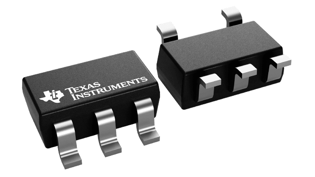
封裝資訊
| 封裝 | 針腳 SOT-23 (DBV) | 5 |
| 操作溫度範圍 (°C) 0 to 70 |
| 包裝數量 | 運送業者 250 | SMALL T&R |
TLV2211 的特色
- Output Swing Includes Both Supply Rails
- Low Noise...21 nV/
 Hz Typ at f = 1 kHz
 - Low Input Bias Current...1 pA Typ
- Very Low Power...11 µA Per Channel Typ
- Common-Mode Input Voltage Range Includes Negative Rail
- Wide Supply Voltage Range 2.7 V to 10 V
- Available in the SOT-23 Package
- Macromodel Included
Advanced LinCMOS is a trademark of Texas Instruments.
TLV2211 的說明
The TLV2211 is a single low-voltage operational amplifier available in the SOT-23 package. It consumes only 11 µA (typ) of supply current and is ideal for battery-power applications. The TLV2211 has a 3-V noise level of 22 nV/ Hz at 1kHz; 5 times lower than competitive SOT-23 micropower solutions. The device exhibits rail-to-rail output performance for increased dynamic range in single- or split-supply applications. The TLV2211 is fully characterized at 3 V and 5 V and is optimized for low-voltage applications.
The TLV2211, exhibiting high input impedance and low noise, is excellent for small-signal conditioning for high-impedance sources, such as piezoelectric transducers. Because of the micropower dissipation levels combined with 3-V operation, these devices work well in hand-held monitoring and remote-sensing applications. In addition, the rail-to-rail output feature with single or split supplies makes this family a great choice when interfacing with analog-to-digital converters (ADCs).
With a total area of 5.6mm2, the SOT-23 package only requires one-third the board space of the standard 8-pin SOIC package. This ultra-small package allows designers to place single amplifiers very close to the signal source, minimizing noise pick-up from long PCB traces. TI has also taken special care to provide a pinout that is optimized for board layout. Both inputs are separated by GND to prevent coupling or leakage paths. The OUT and IN- terminals are on the same end of the board to provide negative feedback. Finally, gain setting resistors and decoupling capacitor are easily placed around the package.