Packaging information
| Package | Pins VQFN (RGZ) | 48 |
| Operating temperature range (°C) -40 to 85 |
| Package qty | Carrier 2,500 | LARGE T&R |
Features for the ADC32J45
- Dual Channel
- 14-Bit Resolution
- Single Supply: 1.8 V
- Flexible Input Clock Buffer with Divide-by-1, -2, -4
- SNR = 72.2 dBFS, SFDR = 87 dBc at
fIN = 70 MHz - Ultralow Power Consumption:
- 227 mW/Ch at 160 MSPS
- Channel Isolation: 105 dB
- Internal Dither
- JESD204B Serial Interface:
- Subclass 0, 1, 2 Compliant up to 3.2 Gbps
- Supports One Lane per ADC up to 160 MSPS
- Support for Multichip Synchronization
- Pin-to-Pin Compatible with 12-Bit Version
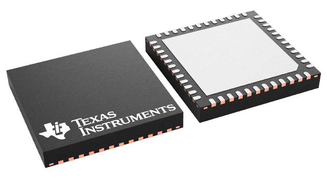
(ADC32J2X) - Package: VQFN-48 (7 mm × 7 mm)
Description for the ADC32J45
The ADC32J4x are a high-linearity, ultra-low power, dual-channel, 14-bit, 50-MSPS to 160-MSPS, analog-to-digital converter (ADC) family. The devices are designed specifically to support demanding, high input frequency signals with large dynamic range requirements. A clock input divider allows more flexibility for system clock architecture design and the SYSREF input enables complete system synchronization. The ADC32J4x family supports JESD204B interface in order to reduce the number of interface lines, thus allowing high system integration density. The JESD204B interface is a serial interface, where the data of each ADC are serialized and output over only one differential pair. An internal phase-locked loop (PLL) multiplies the incoming ADC sampling clock by 20 to derive the bit clock, which is used to serialize the 14-bit data from each channel. The devices support subclass 1 with interface speeds up to 3.2 Gbps.