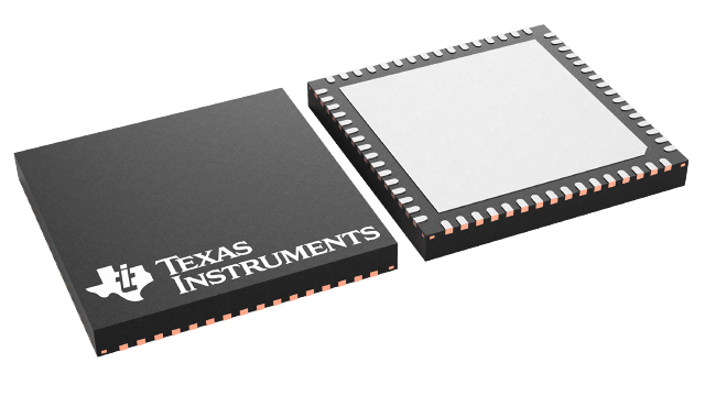
Packaging information
| Package | Pins VQFN (RGC) | 64 |
| Operating temperature range (°C) -40 to 85 |
| Package qty | Carrier 250 | SMALL T&R |
Features for the ADS54J54
- 4 Channel, 14-Bit 500 MSPS ADC
- Analog input buffer with high impedance input
- Flexible input clock buffer with divide by 1/2/4
- 1.25 VPP Differential full-scale input
- JESD204B Serial interface
- Subclass 1 compliant up to 5 Gbps
- 1 Lane Per ADC up to 250 Msps
- 2 Lanes Per ADC up to 500 Msps
- 64-Pin QFN Package (9 mm x 9 mm)
- Key specifications:
- Power dissipation: 875 mW/ch
- Input bandwidth (3 dB): 900 MHz
- Aperture jitter: 98 fs rms
- Channel isolation: 85 dB
- Performance at ƒin = 170 MHz at 1.25
VPP,
1lane 2x Decimation –1 dBFS- SNR: 67.2 dBFS
- SFDR: 85 dBc HD2,3; 95 dBFS non-HD2,3
- Performance at ƒin = 370 MHz at 1.25
VPP,
2lane no Decimation –1 dBFS- SNR: 64.7 dBFS
- SFDR: 75 dBc HD2,3; 83 dBFS non-HD2,3
Description for the ADS54J54
The ADS54J54 is a low power, wide bandwidth 14-bit 500 MSPS quad channel analog-to-digital converter (ADC). It supports the JESD204B serial interface with data rates up to 5 Gbps supporting 1 or 2 lanes per ADC. The buffered analog input provides uniform input impedance across a wide frequency range while minimizing sample-and-hold glitch energy. A sampling clock divider allows more flexibility for system clock architecture design. The ADS54J54 provides excellent spurious-free dynamic range (SFDR) over a large input frequency range with very low power consumption. Optional 2x Decimation Filter provides high-pass or low-pass filter modes.