Packaging information
| Package | Pins VQFN (RHA) | 40 |
| Operating temperature range (°C) -40 to 105 |
| Package qty | Carrier 2,500 | LARGE T&R |
Features for the CC2541-Q1
- RF
- 2.4-GHz Low Energy Compliant and Proprietary RF Wireless MCU
- Supports Data Rates of 250 kbps, 500 kbps, 1 Mbps, and 2 Mbps
- Excellent Link Budget, Enabling Long-Range Applications Without External Front End
- Programmable Output Power up to 0 dBm
- Excellent
Receiver Sensitivity (–94 dBm at
1 Mbps), Selectivity, and Blocking Performance - Suitable for Systems Targeting Compliance With Worldwide Radio Frequency Regulations: ETSI EN 300 328 and EN 300 440 Class 2 (Europe), FCC CFR47 Part 15 (US), and ARIB STD-T66 (Japan)
- Layout
- Few External Components
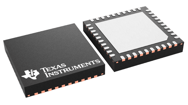
- 6 mm × 6 mm QFN-40 Package
- Low Power
- Active-Mode RX Down to: 18.3 mA
- Active-Mode TX (0 dBm): 18.6 mA
- Power Mode 1 (4-µs Wake-Up): 270 µA
- Power Mode 2 (Sleep Timer On): 1 µA
- Power Mode 3 (External Interrupts): 0.5 µA
- Wide Supply-Voltage Range (2 V to 3.6 V)
- Microcontroller
- High-Performance and Low-Power 8051 Microcontroller Core With Code Prefetch
- 256KB In-System Programmable Flash
- 8KB of RAM With Retention in All Power Modes
- Hardware Debug Support
- Extensive Baseband Automation, Including Auto-Acknowledgment and Address Decoding
- Retention of All Relevant Registers in All Power Modes
- Peripherals
- Powerful Five-Channel DMA
- IR Generation Circuitry
- General-Purpose Timers (One 16-Bit, Two 8-Bit)
- 32-kHz Sleep Timer With Capture
- Accurate Digital RSSI Support
- Battery Monitor and Temperature Sensor
- 12-Bit ADC With Eight Channels and Configurable Resolution
- AES Security Coprocessor
- Two Powerful USARTs With Support for Several Serial Protocols
- 23 General-Purpose I/O Pins
(21 × 4 mA, 2 × 20 mA) - I2C interface
- 2 I/O Pins Have LED Driving Capabilities
- Watchdog Timer
- Integrated High-Performance Comparator
- Development
Tools
- CC2541 Evaluation Module
- SmartRF™ Software
- IAR Embedded Workbench™ Available
- v4.0 Compliant Protocol Stack for Single-Mode BLE
Solution
- Complete Power-Optimized Stack, Including Controller and
Host
- GAP – Central, Peripheral, Observer, or Broadcaster (Including Combination Roles)
- ATT / GATT – Client and Server
- SMP – AES-128 Encryption and Decryption
- L2CAP
- Sample
Applications and Profiles
- Generic Applications for GAP Central and Peripheral Roles
- Proximity, Accelerometer, Simple Keys, and Battery GATT Services
- More Applications Supported in BLE Software Stack
- Multiple Configuration
Options
- Single-Chip Configuration, Allowing Applications to Run on CC2541-Q1
- Network Processor Interface for Applications Running on an External Microcontroller
- BTool–Windows PC Application for Evaluation, Development, and Test
- Over the Air Update Capable
- Complete Power-Optimized Stack, Including Controller and
Host
Description for the CC2541-Q1
The CC2541-Q1 is a power-optimized true Wireless MCU solution for both low energy and proprietary 2.4-GHz applications. This device enables the building of robust nework nodes with low total bill-of-material costs. The CC2541-Q1 combines the excellent performance of a leading RF transceiver with an industry-standard enhanced 8051 MCU, in-system programmable flash memory, 8KB of RAM, and many other powerful supporting features and peripherals. The CC2541-Q1 is highly suited for systems in which ultralow power consumption is required, which is specified by various operating modes. Short transition times between operating modes further enable low power consumption.
The CC2541-Q1 comes in a 6 mm x 6 mm QFN40 package.