SLVSF06 March 2019 TPS65653-Q1
PRODUCT PREVIEW Information. Product in design phase of development. Subject to change or discontinuance without notice.
- 1 Features
- 2 Applications
- 3 Description
- 4 Revision History
- 5 Pin Configuration and Functions
- 6 Specifications
-
7 Detailed Description
- 7.1 Overview
- 7.2 Functional Block Diagram
- 7.3
Feature Description
- 7.3.1 DC/DC Converters
- 7.3.2 Sync Clock Functionality
- 7.3.3 Power-Up
- 7.3.4 Regulator Control
- 7.3.5 Enable and Disable Sequences
- 7.3.6 Device Reset Scenarios
- 7.3.7 Diagnosis and Protection Features
- 7.3.8 Operation of the GPO Signals
- 7.3.9 Digital Signal Filtering
- 7.4 Device Functional Modes
- 7.5 Programming
- 7.6
Register Maps
- 7.6.1
Register Descriptions
- 7.6.1.1 DEV_REV
- 7.6.1.2 OTP_REV
- 7.6.1.3 BUCK0_CTRL_1
- 7.6.1.4 BUCK0_CTRL_2
- 7.6.1.5 BUCK1_CTRL_1
- 7.6.1.6 BUCK1_CTRL_2
- 7.6.1.7 BUCK0_VOUT
- 7.6.1.8 BUCK1_VOUT
- 7.6.1.9 BUCK0_DELAY
- 7.6.1.10 BUCK1_DELAY
- 7.6.1.11 GPO_DELAY
- 7.6.1.12 GPO2_DELAY
- 7.6.1.13 GPO_CTRL
- 7.6.1.14 CONFIG
- 7.6.1.15 PLL_CTRL
- 7.6.1.16 PGOOD_CTRL_1
- 7.6.1.17 PGOOD_CTRL_2
- 7.6.1.18 PG_FAULT
- 7.6.1.19 RESET
- 7.6.1.20 INT_TOP_1
- 7.6.1.21 INT_TOP_2
- 7.6.1.22 INT_BUCK
- 7.6.1.23 TOP_STAT
- 7.6.1.24 BUCK_STAT
- 7.6.1.25 TOP_MASK_1
- 7.6.1.26 TOP_MASK_2
- 7.6.1.27 BUCK_MASK
- 7.6.1.28 SEL_I_LOAD
- 7.6.1.29 I_LOAD_2
- 7.6.1.30 I_LOAD_1
- 7.6.1
Register Descriptions
- 8 Application and Implementation
- 9 Power Supply Recommendations
- 10Layout
- 11Device and Documentation Support
Package Options
Mechanical Data (Package|Pins)
- RHD|28
Thermal pad, mechanical data (Package|Pins)
- RHD|28
Orderable Information
7.3.7.1.1 PGOOD Pin Gated mode
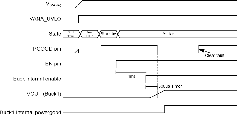
The gated (or unusual) mode of operation is selected by setting PGOOD_MODE bit to 0 in PGOOD_CTRL_2 register.
For the gated mode of operation, PGOOD behaves as follows:
- PGOOD is set to active or asserted state upon exiting OTP configuration as an initial default state.
- PGOOD status is suspended or unchanged during an 800-µs gated time period, thereby gating-off the status indication.
- During normal power-up sequencing and requested voltage changes, PGOOD state is not changed during an 800-µs gated time period. It typically remains active or asserted for normal conditions.
- During an abnormal power-up sequencing and requested voltage changes, PGOOD status could change to inactive or de-asserted after an 800-µs gated time period if any output voltage is outside of regulation range.
- Using the gated mode of operation could allow the PGOOD signal to initiate an immediate power shutdown sequence if the PGOOD signal is wired-OR with signal connected to EN input. This type of circuit configuration provides a smart PORz function for processor that eliminates the need for additional components to generate PORz upon start-up and to monitor voltage levels of key voltage domains.
The fault sets corresponding fault bit 1 in PG_FAULT register. The detected fault must be cleared to continue the PGOOD monitoring. The overvoltage and thermal shutdown are cleared by writing 1 to the OVP_INT and TDIE_SD_INT interrupt bits in INT_TOP_1 register. The regulator fault is cleared by writing 1 to the corresponding register bit in PG_FAULT register. The interrupts can be also cleared with VANA UVLO by toggling the input supply. An example of PGOOD pin operation in gated mode is shown in Figure 11.
 Figure 11. PGOOD Pin Operation in Gated Mode