SLVSF06 March 2019 TPS65653-Q1
PRODUCT PREVIEW Information. Product in design phase of development. Subject to change or discontinuance without notice.
- 1 Features
- 2 Applications
- 3 Description
- 4 Revision History
- 5 Pin Configuration and Functions
- 6 Specifications
-
7 Detailed Description
- 7.1 Overview
- 7.2 Functional Block Diagram
- 7.3
Feature Description
- 7.3.1 DC/DC Converters
- 7.3.2 Sync Clock Functionality
- 7.3.3 Power-Up
- 7.3.4 Regulator Control
- 7.3.5 Enable and Disable Sequences
- 7.3.6 Device Reset Scenarios
- 7.3.7 Diagnosis and Protection Features
- 7.3.8 Operation of the GPO Signals
- 7.3.9 Digital Signal Filtering
- 7.4 Device Functional Modes
- 7.5 Programming
- 7.6
Register Maps
- 7.6.1
Register Descriptions
- 7.6.1.1 DEV_REV
- 7.6.1.2 OTP_REV
- 7.6.1.3 BUCK0_CTRL_1
- 7.6.1.4 BUCK0_CTRL_2
- 7.6.1.5 BUCK1_CTRL_1
- 7.6.1.6 BUCK1_CTRL_2
- 7.6.1.7 BUCK0_VOUT
- 7.6.1.8 BUCK1_VOUT
- 7.6.1.9 BUCK0_DELAY
- 7.6.1.10 BUCK1_DELAY
- 7.6.1.11 GPO_DELAY
- 7.6.1.12 GPO2_DELAY
- 7.6.1.13 GPO_CTRL
- 7.6.1.14 CONFIG
- 7.6.1.15 PLL_CTRL
- 7.6.1.16 PGOOD_CTRL_1
- 7.6.1.17 PGOOD_CTRL_2
- 7.6.1.18 PG_FAULT
- 7.6.1.19 RESET
- 7.6.1.20 INT_TOP_1
- 7.6.1.21 INT_TOP_2
- 7.6.1.22 INT_BUCK
- 7.6.1.23 TOP_STAT
- 7.6.1.24 BUCK_STAT
- 7.6.1.25 TOP_MASK_1
- 7.6.1.26 TOP_MASK_2
- 7.6.1.27 BUCK_MASK
- 7.6.1.28 SEL_I_LOAD
- 7.6.1.29 I_LOAD_2
- 7.6.1.30 I_LOAD_1
- 7.6.1
Register Descriptions
- 8 Application and Implementation
- 9 Power Supply Recommendations
- 10Layout
- 11Device and Documentation Support
Package Options
Mechanical Data (Package|Pins)
- RHD|28
Thermal pad, mechanical data (Package|Pins)
- RHD|28
Orderable Information
7.5.1.3 Transferring Data
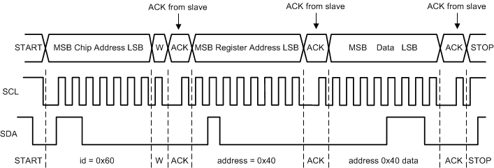
Every byte put on the SDA line must be eight bits long, with the most significant bit (MSB) being transferred first. Each byte of data has to be followed by an acknowledge bit. The acknowledge related clock pulse is generated by the master. The master releases the SDA line (HIGH) during the acknowledge clock pulse. The TPS65653-Q1 pulls down the SDA line during the 9th clock pulse, signifying an acknowledge. The TPS65653-Q1 generates an acknowledge after each byte has been received.
There is one exception to the acknowledge after every byte rule. When the master is the receiver, it must indicate to the transmitter an end of data by not-acknowledging (negative acknowledge) the last byte clocked out of the slave. This negative acknowledge still includes the acknowledge clock pulse (generated by the master), but the SDA line is not pulled down.
NOTE
If the V(VANA) voltage is below VANAUVLO threshold level during I2C communication the TPS65653-Q1 device does not drive SDA line. The ACK signal and data transfer to the master is disabled at that time.
After the START condition, the bus master sends a chip address. This address is seven bits long followed by an eighth bit which is a data direction bit (READ or WRITE). For the eighth bit, a 0 indicates a WRITE, and a 1 indicates a READ. The second byte selects the register to which the data will be written. The third byte contains data to write to the selected register.
 Figure 19. Write Cycle (w = write; SDA = 0). Example Device Address = 0x60