DLPU040B October 2016 – March 2023 DLP650LNIR , DLPC410
- DLP Discovery 4100 Development Platform User’s Guide
- Trademarks
- 1Introduction
-
2Overview
- 2.1 The DLP Discovery 4100 Development Platform
- 2.2 DLP Discovery 4100 Development Platform Photo
- 2.3
Key Components
- 2.3.1 Xilinx Virtex 5 APPSFPGA
- 2.3.2 DLPC410 - Digital Controller for DLP Discovery 4100 Chipset
- 2.3.3 DLPA200 - DMD Micromirror Driver
- 2.3.4 DLPR410 - Configuration PROM for DLPC410 Controller
- 2.3.5 APPSFPGA Flash Configuration PROM
- 2.3.6 DMD Connectors
- 2.3.7 USB Controller
- 2.3.8 50-MHz Oscillator
- 2.3.9 DDR2 SODIMM Connector
- 2.3.10 Connectors
- 2.3.11 Battery
- 2.3.12 Power Supplies
-
3Hardware Overview and Setup
- 3.1 Getting Started
- 3.2
User Connectors and I/O
- 3.2.1 J12 Input Power Connector
- 3.2.2 J18 Input Power Connector
- 3.2.3 J1 USB Connector Pinout
- 3.2.4 J3 USB GPIO
- 3.2.5 J6 GPIO_A Connector
- 3.2.6 J8 DLPC410 Mictor Connector
- 3.2.7 J9 USB/APPSFPGA Mictor Connector
- 3.2.8 J13 DMD Flex 1 Connector
- 3.2.9 J14 DMD Flex 2 Connector
- 3.2.10 J15 DDR2 SODIMM Connector
- 3.2.11 J16, J17 EXP Connectors
- 3.2.12 H1 Xilinx FPGA JTAG Header
- 3.3 Configuration Jumpers
- 3.4 Switches
- 3.5 Power and Status LEDs
- 3.6 Test Points
-
4Software
- 4.1 Overview
- 4.2 DLP Discovery 4100 Operation
- 4.3 Graphical User Interface
- 4.4 Script and Status Operations
- 4.5 DLPC410 Control Window
- 4.6 Test Patterns Window
- 4.7 About Box
- 4.8 Links
- 5Related Documentation
- 6Appendix
- 7Revision History
4.3.3.1 Load Tab
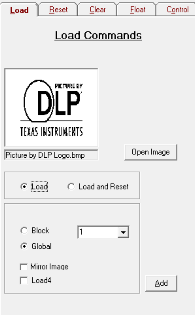
Load commands select the image file and specify load operations.
An image file must be selected before the Add button is pressed. To select an image file click the Open Image button and select the image file. Supported image file types are .bmp, .jpg, .gif and .bin. A .bin file is a binary file containing one bit per DMD pixel. TI recommends to use the initial 24 bit (non-binary) images and let GUI do the conversion to binary image to avoid error due to any unrecognized image format.
The image data can be loaded to DMD memory by selecting Load or the image data can be loaded and the DMD reset to display the image by selecting Load and Reset. If Load and Reset is not selected the image is not visible until a separate Reset command is executed.
The entire image can be loaded (Global) or individual blocks can be loaded (Block). Block numbers can be from 1 to 16. Loading block 16 on a DLP9500 (0.95 1080p) DMD is ignored since this DMD has only 15 blocks.
The image can be mirrored in the horizontal direction by selecting Mirror Image.
The DMD incorporates the Load4 operation to write 4 rows simultaneously with the same column data. This allows fast loading since only 1/4th of actual image data need to be sent to DMD. Load4 option can be selected to enable this mode.
Select the desired options and Add button to add the command to the script.
 Figure 4-22 Load Tab