DLPU040B October   2016  – March 2023 DLP650LNIR , DLPC410


  1.   DLP Discovery 4100 Development Platform User’s Guide
  2.   Trademarks
  3. 1Introduction
    1. 1.1 Welcome
  4. 2Overview
    1. 2.1 The DLP Discovery 4100 Development Platform
    2. 2.2 DLP Discovery 4100 Development Platform Photo
    3. 2.3 Key Components
      1. 2.3.1  Xilinx Virtex 5 APPSFPGA
      2. 2.3.2  DLPC410 - Digital Controller for DLP Discovery 4100 Chipset
      3. 2.3.3  DLPA200 - DMD Micromirror Driver
      4. 2.3.4  DLPR410 - Configuration PROM for DLPC410 Controller
      5. 2.3.5  APPSFPGA Flash Configuration PROM
      6. 2.3.6  DMD Connectors
      7. 2.3.7  USB Controller
      8. 2.3.8  50-MHz Oscillator
      9. 2.3.9  DDR2 SODIMM Connector
      10. 2.3.10 Connectors
        1. 2.3.10.1 JTAG Header H1
        2. 2.3.10.2 Mictor Connectors
        3. 2.3.10.3 GPIO Connectors
      11. 2.3.11 Battery
      12. 2.3.12 Power Supplies
        1. 2.3.12.1 J14 Power Connector
        2. 2.3.12.2 J14 Power Connector
        3. 2.3.12.3 REG. 0.9 V
        4. 2.3.12.4 REG. 1.0 V
        5. 2.3.12.5 REG. 1.8 V
        6. 2.3.12.6 REG. 2.5 V
        7. 2.3.12.7 REG. 3.3 V
        8. 2.3.12.8 REG. 12 V
  5. 3Hardware Overview and Setup
    1. 3.1 Getting Started
    2. 3.2 User Connectors and I/O
      1. 3.2.1  J12 Input Power Connector
      2. 3.2.2  J18 Input Power Connector
      3. 3.2.3  J1 USB Connector Pinout
      4. 3.2.4  J3 USB GPIO
      5. 3.2.5  J6 GPIO_A Connector
      6. 3.2.6  J8 DLPC410 Mictor Connector
      7. 3.2.7  J9 USB/APPSFPGA Mictor Connector
      8. 3.2.8  J13 DMD Flex 1 Connector
      9. 3.2.9  J14 DMD Flex 2 Connector
      10. 3.2.10 J15 DDR2 SODIMM Connector
      11. 3.2.11 J16, J17 EXP Connectors
      12. 3.2.12 H1 Xilinx FPGA JTAG Header
    3. 3.3 Configuration Jumpers
      1. 3.3.1 J2 – EXP Voltage Select
      2. 3.3.2 J4 – APPSFPGA Revision Select
      3. 3.3.3 J5 – Shared USB Signal Enable/Disable
      4. 3.3.4 J7 – USB EEPROM Programming Header
      5. 3.3.5 J10 – DLPA200 B Output Enable
    4. 3.4 Switches
      1. 3.4.1 SW1 - APPSFPGA Functional Switches
      2. 3.4.2 SW2 - APPSFPGA Reset
      3. 3.4.3 SW3 - DMD Power Float (Park)
      4. 3.4.4 SW4 - Input Power On/Off
    5. 3.5 Power and Status LEDs
      1. 3.5.1 D1 – USB Connection Indicator
      2. 3.5.2 D2 and D16 – APPSFPGA Done
      3. 3.5.3 D3 and D17 – DLPC410 Done
      4. 3.5.4 D9 – DDC_LED0
      5. 3.5.5 D10 – DDC_LED1
      6. 3.5.6 D11 – VLED0
      7. 3.5.7 D12 – VLED1
    6. 3.6 Test Points
  6. 4Software
    1. 4.1 Overview
      1. 4.1.1 Software Overview
        1. 4.1.1.1 DMD Image Control
        2. 4.1.1.2 Image Commands
    2. 4.2 DLP Discovery 4100 Operation
      1. 4.2.1 Quick Start Guide on Operation
      2. 4.2.2 74
    3. 4.3 Graphical User Interface
      1. 4.3.1 Menu Bar
        1. 4.3.1.1 File Menu
        2. 4.3.1.2 View Menu
        3. 4.3.1.3 DMD Menu
        4. 4.3.1.4 Execution Menu
        5. 4.3.1.5 Test Patterns Menu
        6. 4.3.1.6 Help Menu
      2. 4.3.2 Toolbar
        1. 4.3.2.1 File Menu Buttons
        2. 4.3.2.2 Run, Run Once, Loop Break, Step and Stop Controls
        3. 4.3.2.3 Set Start and End Buttons
        4. 4.3.2.4 Help Button
      3. 4.3.3 Script Commands Window
        1. 4.3.3.1 Load Tab
        2. 4.3.3.2 Reset Tab
        3. 4.3.3.3 Clear Tab
        4. 4.3.3.4 Float Tab
        5. 4.3.3.5 Control Tab
      4. 4.3.4 Status Window
      5. 4.3.5 Script Window
        1. 4.3.5.1 Inserting Commands
        2. 4.3.5.2 Moving Commands
        3. 4.3.5.3 Deleting Commands
    4. 4.4 Script and Status Operations
      1. 4.4.1 Saving Scripts and Statuses
        1. 4.4.1.1 Saving a Script
        2. 4.4.1.2 Saving a Status
      2. 4.4.2 Printing Scripts and Statuses
        1. 4.4.2.1 Printing a Script
        2. 4.4.2.2 Printing a Status
      3. 4.4.3 Opening Scripts and Statuses
      4. 4.4.4 Creating New Scripts and Statuses
        1. 4.4.4.1 Creating a New Script
        2. 4.4.4.2 Creating a New Status
    5. 4.5 DLPC410 Control Window
    6. 4.6 Test Patterns Window
    7. 4.7 About Box
    8. 4.8 Links
  7. 5Related Documentation
  8. 6Appendix
    1. 6.1 Abbreviations and Acronyms
    2. 6.2 Notational Conventions
      1. 6.2.1 Information About Cautions and Warnings
  9. 7Revision History

Clear Tab

The Clear Tab commands clear the memory contents of all the blocks using the Global option or individually using the Single Block option by writing zeroes to the contents of DMD memory. The Clear option clears memory only, the Clear and Reset option clears memory and performs a reset to change the display. Select the desired option and click on the Add button to add to script (see #DLPU0403191).

Note: NOTE: The Global option is implemented in software by sequentially issuing a DMD Block Clear command to all the blocks on the DMD.
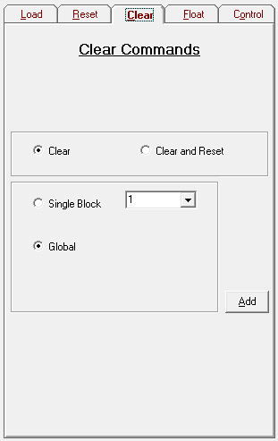
GUID-78706653-6B32-40A0-A3B6-0C04CB66AFA6-low.pngFigure 4-24 Clear Tab