DLPU040B October 2016 – March 2023 DLP650LNIR , DLPC410
- DLP Discovery 4100 Development Platform User’s Guide
- Trademarks
- 1Introduction
-
2Overview
- 2.1 The DLP Discovery 4100 Development Platform
- 2.2 DLP Discovery 4100 Development Platform Photo
- 2.3
Key Components
- 2.3.1 Xilinx Virtex 5 APPSFPGA
- 2.3.2 DLPC410 - Digital Controller for DLP Discovery 4100 Chipset
- 2.3.3 DLPA200 - DMD Micromirror Driver
- 2.3.4 DLPR410 - Configuration PROM for DLPC410 Controller
- 2.3.5 APPSFPGA Flash Configuration PROM
- 2.3.6 DMD Connectors
- 2.3.7 USB Controller
- 2.3.8 50-MHz Oscillator
- 2.3.9 DDR2 SODIMM Connector
- 2.3.10 Connectors
- 2.3.11 Battery
- 2.3.12 Power Supplies
-
3Hardware Overview and Setup
- 3.1 Getting Started
- 3.2
User Connectors and I/O
- 3.2.1 J12 Input Power Connector
- 3.2.2 J18 Input Power Connector
- 3.2.3 J1 USB Connector Pinout
- 3.2.4 J3 USB GPIO
- 3.2.5 J6 GPIO_A Connector
- 3.2.6 J8 DLPC410 Mictor Connector
- 3.2.7 J9 USB/APPSFPGA Mictor Connector
- 3.2.8 J13 DMD Flex 1 Connector
- 3.2.9 J14 DMD Flex 2 Connector
- 3.2.10 J15 DDR2 SODIMM Connector
- 3.2.11 J16, J17 EXP Connectors
- 3.2.12 H1 Xilinx FPGA JTAG Header
- 3.3 Configuration Jumpers
- 3.4 Switches
- 3.5 Power and Status LEDs
- 3.6 Test Points
-
4Software
- 4.1 Overview
- 4.2 DLP Discovery 4100 Operation
- 4.3 Graphical User Interface
- 4.4 Script and Status Operations
- 4.5 DLPC410 Control Window
- 4.6 Test Patterns Window
- 4.7 About Box
- 4.8 Links
- 5Related Documentation
- 6Appendix
- 7Revision History
2.1 The DLP Discovery 4100 Development Platform
The DLP Discovery 4100 Development Platform (D4100 Platform) typically refers to the combination of one DLPLCRC410EVM plus one DMD EVM. Together these include:
- 1 ea. DLPLCRC410EVM Controller Board
- 1 ea. DMD board with DMD and DMD mounting mechanics (Type-A DMDs only)
- 1 ea. or 2 ea. flexible PCB cables
Not included in the kit but needed for operation are:
- 1 ea. Power supply: VOUT = 5 V, IOUT = 6 A (required)
Not included, optional and only needed if developing and downloading new APPSFPGA firmware:
- 1 ea. Xilinx DLC9G programming cable.
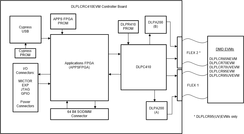
#T4709747-27 is a simplified block diagram of the D4100 Platform.
 Figure 2-1 D4100 Platform Diagram
The DLP Discovery 4100 EVM Controller Board of the DLPLCRC410EVM contains:
- DLPC410 DLP Digital Controller
- Provides input high speed 16/32/64 bit 2xLVDS data and control user interface.
- Provides output data and control interface to the DMD and DLPA200s.
- DLPR410 Configuration PROM
- Stores and provides configuration data for the DLPC410 controller.
- DLPA200 DMD Micromirror Driver
- Generates Mirror Clocking Pulses (Resets) for up to 16 DMD Reset Blocks.
- Supports high reset frequencies.
- One required for DLP650LNIR, DLP7000, or DLP7000UV DMDs, and two for DLP9500, DLP9500UV DMDs.
- 16/32/64-bit 400 MHz 2xLVDS DLPC410 to DMD Data Interface
- 16 bits used for the DLP650LNIR DMD.
- 32 bits used for the DLP7000 and DLP7000UV DMDs.
- 64 bits used for the DLP9500 and DLP9500UV DMDs.
- 5 Volt input power connector
- On-board regulation of other power supplies included.
- Applications FPGA (APPSFPGA)
- Xilinx Virtex 5 (XC5VLX50) FPGA for user application pattern generation and development opportunities.
- APPSFPGA Configuration PROM (XCF16P)
- Stores and provides configuration data for the APPSFPGA. User programmable for future development.
- A 64-bit DDR2 SODIMM connector
- For end user development of image storage.
- A Cypress CY7C68013A USB controller
- Provides USB data and control interface (USB speeds can limit pattern rates).
- Enabled end user development of USB interface.
- EXP Expansion Connectors
- Connect to external EXP interface compatible customer boards.
- Includes additional 2xLVDS pairs to support 64 bit 2xLVDS connection through EXP connectors.
- Flash Memory (connected to APPSFPGA)
- Non-volatile storage for end user development.
- Various I/O connectors
- Mictor test connectors for logic analyzer connection.
- JTAG headers for device programming.
- GPIO connectors for general purpose digital I/O.