JAJU732C June   2019  – July 2022


  1.   概要
  2.   Resources
  3.   特長
  4.   アプリケーション
  5.   5
  6. 1System Description
    1. 1.1 Key System Specifications
  7. 2System Overview
    1. 2.1 Block Diagram
    2. 2.2 Highlighted Products
      1. 2.2.1  UCC21530
      2. 2.2.2  AMC1311
      3. 2.2.3  AMC3302
      4. 2.2.4  AMC3306M05
      5. 2.2.5  LM76003
      6. 2.2.6  LMZ31707
      7. 2.2.7  OPA320
      8. 2.2.8  ISO7721
      9. 2.2.9  SN6501
      10. 2.2.10 SN6505B
      11. 2.2.11 TMP235
      12. 2.2.12 LMT87
      13. 2.2.13 TL431
      14. 2.2.14 LMV762
      15. 2.2.15 TMS320F280049 C2000 MCU
      16. 2.2.16 TMDSCNCD280049C
    3. 2.3 System Design Theory
      1. 2.3.1 Dual Active Bridge Analogy With Power Systems
      2. 2.3.2 Dual-Active Bridge - Switching Sequence
      3. 2.3.3 Dual-Active Bridge - Zero Voltage Switching (ZVS)
      4. 2.3.4 Dual-Active Bridge - Design Considerations
        1. 2.3.4.1 Leakage Inductor
        2. 2.3.4.2 Effect of Inductance on Current
        3. 2.3.4.3 Phase Shift
        4. 2.3.4.4 Capacitor Selection
        5. 2.3.4.5 Soft Switching Range
        6. 2.3.4.6 Switching Frequency
        7. 2.3.4.7 Transformer Selection
        8. 2.3.4.8 SiC MOSFET Selection
      5. 2.3.5 Loss Analysis
        1. 2.3.5.1 Design Equations
        2. 2.3.5.2 SiC MOSFET and Diode Losses
        3. 2.3.5.3 Transformer Losses
        4. 2.3.5.4 Inductor Losses
        5. 2.3.5.5 Gate Driver Losses
        6. 2.3.5.6 Efficiency
        7. 2.3.5.7 Thermal Considerations
  8. 3Circuit Description
    1. 3.1 Power Stage
    2. 3.2 DC Voltage Sensing
      1. 3.2.1 Primary DC Voltage Sensing
      2. 3.2.2 Secondary DC Voltage Sensing
    3. 3.3 Current Sensing
    4. 3.4 Power Architecture
      1. 3.4.1 Auxiliary Power Supply
      2. 3.4.2 Isolated Power Supply for Sense Circuits
    5. 3.5 Gate Driver
      1. 3.5.1 Gate Driver Circuit
      2. 3.5.2 Gate Driver Bias Power Supply
      3. 3.5.3 Gate Driver Discrete Circuits - Short-Circuit Detection and Two Level Turn Off
  9. 4Hardware, Software, Testing Requirements, and Test Results
    1. 4.1 Required Hardware and Software
      1. 4.1.1 Hardware
      2. 4.1.2 Software
        1. 4.1.2.1 Getting Started With Software
        2. 4.1.2.2 Pin Configuration
        3. 4.1.2.3 PWM Configuration
        4. 4.1.2.4 High-Resolution Phase Shift Configuration
        5. 4.1.2.5 ADC Configuration
        6. 4.1.2.6 ISR Structure
    2. 4.2 Test Setup
    3. 4.3 PowerSUITE GUI
    4. 4.4 LABs
      1. 4.4.1 Lab 1
      2. 4.4.2 Lab 2
      3. 4.4.3 Lab 3
      4. 4.4.4 Lab 4
      5. 4.4.5 Lab 5
    5. 4.5 Test Results
      1. 4.5.1 Open-Loop Performance
      2. 4.5.2 Closed-Loop Performance
  10. 5Design Files
    1. 5.1 Schematics
    2. 5.2 Bill of Materials
    3. 5.3 PCB Layout Recommendations
      1. 5.3.1 Layout Prints
    4. 5.4 Altium Project
    5. 5.5 Gerber Files
    6. 5.6 Assembly Drawings
  11. 6Related Documentation
    1. 6.1 Trademarks
  12. 7Terminology
  13. 8About the Author
  14. 9Revision History

Auxiliary Power Supply

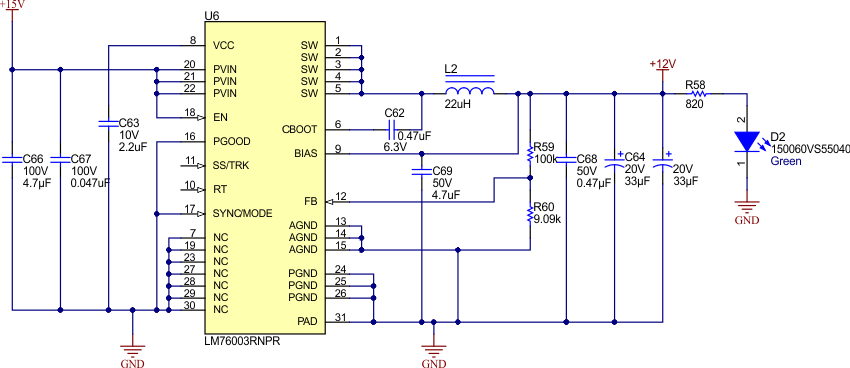
The primary voltage for powering the auxiliary circuits is up to 50 V, which is given as input to the LM76003. The feedback resistors R59 and R60 are configured to provide an output voltage of 12 V. Figure 3-8 shows the LM76003 circuit.

GUID-20210823-SS0I-GLRL-QXJB-CVSRHLKV4MZ5-low.gif

Figure 3-8 LM76003 Circuit

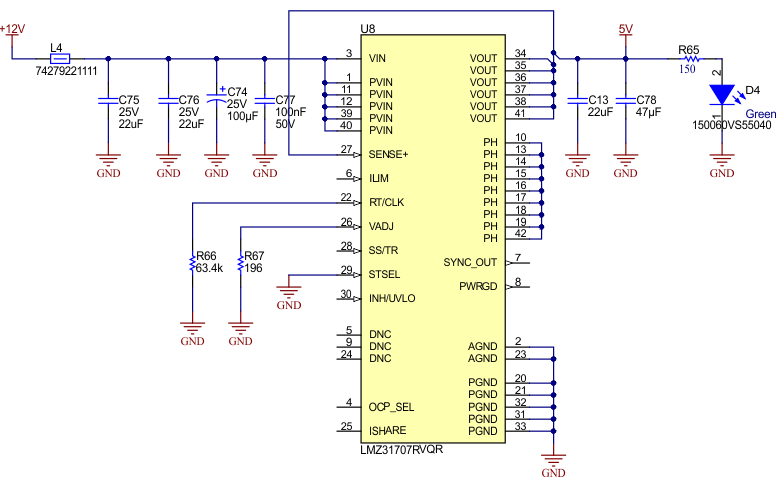
This 12-V rail is used to for cooling fan control and it is further scaled down to 5 V with LMZ31707. The LMZ31707 SIMPLE SWITCHER® power module is an easy-to-use integrated power solution that combines a 7-A DC/DC converter with power MOSFETs, a shielded inductor, and passives into a low profile, QFN package. Figure 3-9 shows the LMZ31707 circuit.

GUID-20210823-SS0I-FNXL-THZ5-5HMM4CHGK7XV-low.gif

Figure 3-9 LMZ31707 Circuit

The other rail voltage of 3.3 V is produced by using the TLV1117LV33. The circuit is shown in Figure 3-10.
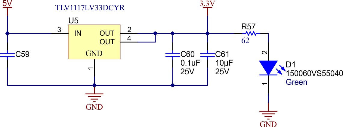
GUID-5C3EACA7-6796-4BF0-B786-61B8CED15093-low.gif Figure 3-10 3.3-V Circuit