JAJU732C June 2019 – July 2022
- 概要
- Resources
- 特長
- アプリケーション
- 5
- 1System Description
- 2System Overview
- 3Circuit Description
- 4Hardware, Software, Testing Requirements, and Test Results
- 5Design Files
- 6Related Documentation
- 7Terminology
- 8About the Author
- 9Revision History
1 System Description
The electric vehicle charging standards governed by the Combined Charging System and CHAdeMO® are constantly changing and are pushing for faster battery charging rates requiring typically less than 30 minutes spent at a charging station for one full charge of an electric vehicle. The DC charging station is typically a Level 3 charger which can cater to a very high power level between 120–240 kW. These DC charging stations are standalone units which house AC/DC and DC/DC power conversion stages. A number of power conversion modules are stacked together inside of a charging station to increase the power levels and enable fast charging. DC fast-charging stations provide a high power DC current to an electric vehicle’s battery without passing through any onboard AC/DC converter, which means the current is connected directly to the battery. Most cars on the road today can handle only up to 50 kW. Newer cars will have the ability to charge at greater rates of power. As EVs come with higher range and batteries get bigger, DC charging solutions are being developed to support long-range EV batteries through fast charging stations up to 250 kW or more.
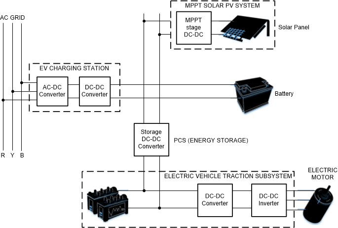
The DC/DC converter in a charging station must be capable of interfacing with the rectified bus voltage (700-800 V) from a three-phase Vienna rectifier at its input and connect with the battery of an electric vehicle at its output, delivering rated power. The DC/DC converter finds important application in a number of end equipment. Figure 1-1 shows its use in charging stations, solar photovoltaic systems, energy storage systems, and electric vehicle traction applications.
 Figure 1-1 Role of DC/DC Converter
The DC/DC converter must be capable of handling high power levels. In addition to this, the converter must be modular, which enables single power stage converter units to be paralleled, whereby the output power throughput can be scaled to higher levels as required by DC charging station standards. Current trends in the charging station are moving toward converters that can handle bidirectional power flow. New practices, such as Vehicle-to-Grid (V2G), involve power transfer between the battery of an electric vehicle and the AC grid. Bidirectional DC/DC converters enable charging of the battery in the forward mode of operation and facilitate flow of power back to the grid from the battery during reverse mode of operation, which can be used to stabilize the grid during peak load periods.
Power density and system efficiency are two important requirements of a converter in a DC charging station. Operating at high switching frequencies enables reduced size of magnetics. By moving to higher bus voltage to facilitate fast charging, more power can be transferred at the same current level. This helps to reduce the amount of copper, thereby improving power density of the converter. The converter must also be highly efficient as it results in significant cost savings and reduced thermal solution. This reduced thermal solution directly translates into reduced and compact heat sink size, which in turn increases the power density of the converter. The converter must also be capable of inherent soft switching like ZVS (Zero Voltage Switching) and ZCS (Zero Current Switching) without the addition any bulky passive components which might hamper power density.
The DC/DC converter must be capable of interfacing seamlessly with Lithium ion or a lead acid battery, which are predominantly used in EV charging stations. The DC/DC converter must also be capable of providing the required voltage conversion between the high-voltage and low-voltage side and provide galvanic isolation between them.
Traditional switching devices have a limit on how quickly they can switch high voltages, or more appropriately, the dV/dt ability of the device. This slow ramping process increases switching loss because the device spends more time in switching transition. This increased switch time also increases the amount of dead time required in the control system to prevent shoot-through and shorts. The solution to this has been developed in newer switching semiconductor technology such as SiC and GaN devices with high electron mobility. This reference design uses SiC MOSFETs alongside TI's SiC gate driver technology to demonstrate the potential benefits it translates when it comes to efficiency and power density.
The following four popular topologies were considered for analysis.
- LLC resonant converter
- Phase-shifted, full bridge
- Single-phase, dual-active bridge
- Dual-active bridge in CLLC mode
Based on this study, the dual-active bridge was chosen for implementation in this reference design, owing to its ease of bidirectional operation, modular structure, competitive efficiency, and power density numbers with respect to other competing topologies. This reference design focuses on addressing the challenges when designing a high-power, dual-active-bridge DC/DC converter for the EV charging station.