JAJU732C June   2019  – July 2022


  1.   概要
  2.   Resources
  3.   特長
  4.   アプリケーション
  5.   5
  6. 1System Description
    1. 1.1 Key System Specifications
  7. 2System Overview
    1. 2.1 Block Diagram
    2. 2.2 Highlighted Products
      1. 2.2.1  UCC21530
      2. 2.2.2  AMC1311
      3. 2.2.3  AMC3302
      4. 2.2.4  AMC3306M05
      5. 2.2.5  LM76003
      6. 2.2.6  LMZ31707
      7. 2.2.7  OPA320
      8. 2.2.8  ISO7721
      9. 2.2.9  SN6501
      10. 2.2.10 SN6505B
      11. 2.2.11 TMP235
      12. 2.2.12 LMT87
      13. 2.2.13 TL431
      14. 2.2.14 LMV762
      15. 2.2.15 TMS320F280049 C2000 MCU
      16. 2.2.16 TMDSCNCD280049C
    3. 2.3 System Design Theory
      1. 2.3.1 Dual Active Bridge Analogy With Power Systems
      2. 2.3.2 Dual-Active Bridge - Switching Sequence
      3. 2.3.3 Dual-Active Bridge - Zero Voltage Switching (ZVS)
      4. 2.3.4 Dual-Active Bridge - Design Considerations
        1. 2.3.4.1 Leakage Inductor
        2. 2.3.4.2 Effect of Inductance on Current
        3. 2.3.4.3 Phase Shift
        4. 2.3.4.4 Capacitor Selection
        5. 2.3.4.5 Soft Switching Range
        6. 2.3.4.6 Switching Frequency
        7. 2.3.4.7 Transformer Selection
        8. 2.3.4.8 SiC MOSFET Selection
      5. 2.3.5 Loss Analysis
        1. 2.3.5.1 Design Equations
        2. 2.3.5.2 SiC MOSFET and Diode Losses
        3. 2.3.5.3 Transformer Losses
        4. 2.3.5.4 Inductor Losses
        5. 2.3.5.5 Gate Driver Losses
        6. 2.3.5.6 Efficiency
        7. 2.3.5.7 Thermal Considerations
  8. 3Circuit Description
    1. 3.1 Power Stage
    2. 3.2 DC Voltage Sensing
      1. 3.2.1 Primary DC Voltage Sensing
      2. 3.2.2 Secondary DC Voltage Sensing
    3. 3.3 Current Sensing
    4. 3.4 Power Architecture
      1. 3.4.1 Auxiliary Power Supply
      2. 3.4.2 Isolated Power Supply for Sense Circuits
    5. 3.5 Gate Driver
      1. 3.5.1 Gate Driver Circuit
      2. 3.5.2 Gate Driver Bias Power Supply
      3. 3.5.3 Gate Driver Discrete Circuits - Short-Circuit Detection and Two Level Turn Off
  9. 4Hardware, Software, Testing Requirements, and Test Results
    1. 4.1 Required Hardware and Software
      1. 4.1.1 Hardware
      2. 4.1.2 Software
        1. 4.1.2.1 Getting Started With Software
        2. 4.1.2.2 Pin Configuration
        3. 4.1.2.3 PWM Configuration
        4. 4.1.2.4 High-Resolution Phase Shift Configuration
        5. 4.1.2.5 ADC Configuration
        6. 4.1.2.6 ISR Structure
    2. 4.2 Test Setup
    3. 4.3 PowerSUITE GUI
    4. 4.4 LABs
      1. 4.4.1 Lab 1
      2. 4.4.2 Lab 2
      3. 4.4.3 Lab 3
      4. 4.4.4 Lab 4
      5. 4.4.5 Lab 5
    5. 4.5 Test Results
      1. 4.5.1 Open-Loop Performance
      2. 4.5.2 Closed-Loop Performance
  10. 5Design Files
    1. 5.1 Schematics
    2. 5.2 Bill of Materials
    3. 5.3 PCB Layout Recommendations
      1. 5.3.1 Layout Prints
    4. 5.4 Altium Project
    5. 5.5 Gerber Files
    6. 5.6 Assembly Drawings
  11. 6Related Documentation
    1. 6.1 Trademarks
  12. 7Terminology
  13. 8About the Author
  14. 9Revision History

Leakage Inductor

The most important design parameter is the selection of leakage inductor. The power transfer relation of the dual-active bridge is given by Equation 6.

Equation 6. GUID-D830D576-92BB-4207-B257-D181C7530F8B-low.gif

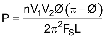
Equation 6 shows that a low value of inductance will lead to high power transfer capability. The maximum value of power transfer for a given switching frequency, leakage inductor, and input and output voltage will occur at
Ø = π/2.

Figure 2-15 shows the inductor current waveform. The value of current at points i1 and i2 can be derived from this waveform.

Equation 7. i 1 = 0.5 2 Ø - 1 - d π I n o m
Equation 8. i 2 = 0.5 2 d Ø + 1 - d π I n o m

Where d is the voltage transfer ratio of the converter given in Equation 9 and Inom is the nominal base current of the converter.

Equation 9. GUID-EE78C879-1A94-444A-960F-D1487BB29C24-low.gif
GUID-ABF655F9-3782-4D8C-AF8C-04689279B6EE-low.gif Figure 2-15 Inductor Current Waveform

From Equation 7 and Equation 8, the conditions for zero voltage switching for leading and lagging bridge of the converter can be obtained.

From the following conditions, the conditions for ZVS are obtained in terms of phase and voltage gain of the converter, summarized in Equation 10 and Equation 11 for the primary bridge and secondary bridges respectively.

  • i1 > 0 for the secondary side bridge
  • i2 > 0 for the primary side bridge
Equation 10. GUID-5B2429C5-EB8B-49EE-BFE1-F449BC5ECDA4-low.gif
Equation 11. GUID-D8E2C14C-B8D9-476A-BAFE-B840FA325EDB-low.gif

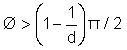
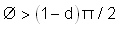
By combining Equation 7, Equation 8, Equation 10, and Equation 11, the relationship between output power and voltage ratio for different values of the inductor is obtained. A MATLAB® script used to plot this relationship is depicted in Figure 2-16. The figure shows that for a particular value of inductance, when the voltage transfer ratio changes from unity, the converter switches experience hard switching. As long as the voltage transfer ratio is kept at unity, soft switching across both the primary and secondary leg switches is obtained. The most important point to note is that the soft switching region (zero voltage switching) depends on the value of leakage inductance. As the value of inductance increases, the ability for soft switching of the converter extends up to very low power levels (light loads).

GUID-91C9A804-0EBE-4AAE-B0CD-A5EAE01A8742-low.gif Figure 2-16 ZVS Range and Output Power Versus Voltage Transfer Ratio