JAJU732C June 2019 – July 2022
- 概要
- Resources
- 特長
- アプリケーション
- 5
- 1System Description
- 2System Overview
- 3Circuit Description
- 4Hardware, Software, Testing Requirements, and Test Results
- 5Design Files
- 6Related Documentation
- 7Terminology
- 8About the Author
- 9Revision History
2.3.5.3 Transformer Losses
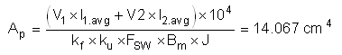
This section provides an estimate of the different components of transformer loss. The transformer for this design was completed with the help of Payton Planar Magnetics®. This reference design focuses only on the loss of numbers and not the actual design process of the transformer. To select the core for this transformer, the area product approach is considered. The area product of the transformer is calculated by Equation 28.
where
- kf is the waveform factor
- ku is the utilization factor
- FSW is the switching frequency
- Bm is the maximum flux density
- J is the current density
- V1 is the primary voltage
- I1.avg is the primary average current
- V2 is the secondary voltage
- I2.avg is the secondary average current
Substitute the values for flux density as 0.2 T, switching frequency as 100 kHz, and utilization factor as 0.3 as this is a planar design. With a waveform factor of 4 and current density as 400 A/cm2, the area product is calculated as 18 cm4. Choosing a core with area product greater than the calculated value, E64/18/50 ferrite DMR44 core was chosen.
Next, the number of turns required for the primary and secondary side is calculated. The number of primary turns is calculated using Equation 29.
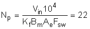
From the data sheet for the core, the effective core area, Ae, is 516 mm2. By substituting this value, the number of turns is approximately 22. In a practical implementation, the number of turns selected in the primary was 24. By using the required conversion ratio of 1.6 between the primary and secondary, the number of secondary turns, Ns, is 15 turns.
Figure 2-24 shows the parameters of the core obtained from the data sheet. The core loss per unit of volume, Pv, at 100°C is approximately 300 mW/cm3. The core volume, Ae, is 81.9 cm2. Therefore, the total core loss at 100 kHz is given by Equation 30.
 Figure 2-24 Transformer Core Data
From the data sheet of the manufacturer, the primary and secondary winding DC resistances were 43 mΩ and 16 mΩ, respectively. The copper losses in the windings were calculated as per Equation 31.

Losses due to the AC resistance at high frequencies are also arising as a result of the skin effect. At 100 kHz, Figure 2-25 shows that the AC resistance is approximately 12.5 mΩ. These contribute 8 W of loss due to current flowing in the primary and secondary windings.
 Figure 2-25 AC Resistance
The core loss, copper losses, and skin effect losses together contribute 50 W of transformer loss. The 10-kW planar transformer designed with Payton is summarized in Table 2-2:
| Functional specifications | Ratings |
|---|---|
| Total output power | 10 kW (500 V/20 Adc) |
| Operating frequency | 100-200 kHz |
| Input voltage of transformer | 800 V (Vout = 500 V), Bipolar Square waveform; |
| Volt-second product | 8000 V μs – for Vout = 500 V, 100 kHz; |
| Primary-to-secondary ratio | 24:15 |
| Primary current maximum | 13.5 Arms (20 A peak) – for Vout = 500 V; |
| Secondary current maximum | 20 Arms (30 A peak) – for Vout = 500 V; |
| Estimated power losses | 50 W – for Vout = 500 V, 100 kHz; |
| Primary winding DC resistance | 43 mΩ |
| Secondary winding DC resistance | 16 mΩ |
| Leakage inductance |
34 µH |
| Magnetizing inductance | 720 µH |
More details of this transformer are available from Payton.