JAJU732C June   2019  – July 2022


  1.   概要
  2.   Resources
  3.   特長
  4.   アプリケーション
  5.   5
  6. 1System Description
    1. 1.1 Key System Specifications
  7. 2System Overview
    1. 2.1 Block Diagram
    2. 2.2 Highlighted Products
      1. 2.2.1  UCC21530
      2. 2.2.2  AMC1311
      3. 2.2.3  AMC3302
      4. 2.2.4  AMC3306M05
      5. 2.2.5  LM76003
      6. 2.2.6  LMZ31707
      7. 2.2.7  OPA320
      8. 2.2.8  ISO7721
      9. 2.2.9  SN6501
      10. 2.2.10 SN6505B
      11. 2.2.11 TMP235
      12. 2.2.12 LMT87
      13. 2.2.13 TL431
      14. 2.2.14 LMV762
      15. 2.2.15 TMS320F280049 C2000 MCU
      16. 2.2.16 TMDSCNCD280049C
    3. 2.3 System Design Theory
      1. 2.3.1 Dual Active Bridge Analogy With Power Systems
      2. 2.3.2 Dual-Active Bridge - Switching Sequence
      3. 2.3.3 Dual-Active Bridge - Zero Voltage Switching (ZVS)
      4. 2.3.4 Dual-Active Bridge - Design Considerations
        1. 2.3.4.1 Leakage Inductor
        2. 2.3.4.2 Effect of Inductance on Current
        3. 2.3.4.3 Phase Shift
        4. 2.3.4.4 Capacitor Selection
        5. 2.3.4.5 Soft Switching Range
        6. 2.3.4.6 Switching Frequency
        7. 2.3.4.7 Transformer Selection
        8. 2.3.4.8 SiC MOSFET Selection
      5. 2.3.5 Loss Analysis
        1. 2.3.5.1 Design Equations
        2. 2.3.5.2 SiC MOSFET and Diode Losses
        3. 2.3.5.3 Transformer Losses
        4. 2.3.5.4 Inductor Losses
        5. 2.3.5.5 Gate Driver Losses
        6. 2.3.5.6 Efficiency
        7. 2.3.5.7 Thermal Considerations
  8. 3Circuit Description
    1. 3.1 Power Stage
    2. 3.2 DC Voltage Sensing
      1. 3.2.1 Primary DC Voltage Sensing
      2. 3.2.2 Secondary DC Voltage Sensing
    3. 3.3 Current Sensing
    4. 3.4 Power Architecture
      1. 3.4.1 Auxiliary Power Supply
      2. 3.4.2 Isolated Power Supply for Sense Circuits
    5. 3.5 Gate Driver
      1. 3.5.1 Gate Driver Circuit
      2. 3.5.2 Gate Driver Bias Power Supply
      3. 3.5.3 Gate Driver Discrete Circuits - Short-Circuit Detection and Two Level Turn Off
  9. 4Hardware, Software, Testing Requirements, and Test Results
    1. 4.1 Required Hardware and Software
      1. 4.1.1 Hardware
      2. 4.1.2 Software
        1. 4.1.2.1 Getting Started With Software
        2. 4.1.2.2 Pin Configuration
        3. 4.1.2.3 PWM Configuration
        4. 4.1.2.4 High-Resolution Phase Shift Configuration
        5. 4.1.2.5 ADC Configuration
        6. 4.1.2.6 ISR Structure
    2. 4.2 Test Setup
    3. 4.3 PowerSUITE GUI
    4. 4.4 LABs
      1. 4.4.1 Lab 1
      2. 4.4.2 Lab 2
      3. 4.4.3 Lab 3
      4. 4.4.4 Lab 4
      5. 4.4.5 Lab 5
    5. 4.5 Test Results
      1. 4.5.1 Open-Loop Performance
      2. 4.5.2 Closed-Loop Performance
  10. 5Design Files
    1. 5.1 Schematics
    2. 5.2 Bill of Materials
    3. 5.3 PCB Layout Recommendations
      1. 5.3.1 Layout Prints
    4. 5.4 Altium Project
    5. 5.5 Gerber Files
    6. 5.6 Assembly Drawings
  11. 6Related Documentation
    1. 6.1 Trademarks
  12. 7Terminology
  13. 8About the Author
  14. 9Revision History

Capacitor Selection

The output capacitor in the dual-active bridge must be designed to handle the ripple. This value impacts the output voltage specification. From Figure 2-19, Equation 15 and Equation 16 are obtained.

Equation 15. GUID-C8416785-4DBA-4F3B-91C5-2731C8381594-low.gif
Equation 16. GUID-C08140C2-E7C0-4AC0-B562-ABEE26F4B294-low.gif
GUID-79502140-E7F7-41DF-82BE-5C87DBC7E342-low.gif
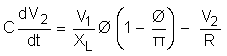
Figure 2-19 Output Current in Dual-Active Bridge

Figure 2-20 shows the effect of the leakage inductor on the selection of the output capacitance. For a particular value of phase shift and inductance, capacitance required for containing the voltage ripple to a specified limit, as per the system specification, increases as the leakage inductor increases. This also means that more capacitance is needed to handle the voltage ripple. As the RMS value of capacitor current increases, more is the loss dissipated across the equivalent series resistance (ESR) of capacitance. Considering these factors, the output capacitor was chosen to keep the output voltage under 5% ripple.

GUID-63C51CFE-3A1A-4808-96D6-A595ED687BCF-low.gifFigure 2-20 Desired Output Capacitance Versus Leakage Inductance