SBASAM0 March 2024 ADS127L18
ADVANCE INFORMATION
- 1
- 1 Features
- 2 Applications
- 3 Description
- 4 Pin Configuration and Functions
- 5 Specifications
-
6 Parameter Measurement Information
- 6.1 Offset Error Measurement
- 6.2 Offset Drift Measurement
- 6.3 Gain Error Measurement
- 6.4 Gain Drift Measurement
- 6.5 NMRR Measurement
- 6.6 CMRR Measurement
- 6.7 PSRR Measurement
- 6.8 SNR Measurement
- 6.9 INL Error Measurement
- 6.10 THD Measurement
- 6.11 IMD Measurement
- 6.12 SFDR Measurement
- 6.13 Noise Performance
-
7 Detailed Description
- 7.1 Overview
- 7.2 Functional Block Diagram
- 7.3 Feature Description
- 7.4 Device Functional Modes
- 7.5 Programming
- 8 Register Map
- 9 Application and Implementation
- 10Device and Documentation Support
- 11Revision History
- 12Mechanical, Packaging, and Orderable Information
Package Options
Mechanical Data (Package|Pins)
- RSH|56
Thermal pad, mechanical data (Package|Pins)
Orderable Information
7.3.9.1 Sinc4 Filter
The sinc4 filter performs averaging and decimation of the modulator data for data rates ranging to 1365.3kSPS in max-speed mode and to 133.333 kSPS in low-speed mode. Increasing the OSR value decreases the ADC data rate and simultaneously reduces signal bandwidth and total noise resulting from increased decimation and data averaging.
The amount of data averaging is reduced for OSR values equal to 12, 16, and 24. Because of this reduction, full 24-bit output data resolution is not available. Table 7-5 summarizes the output data resolution for these OSR values.
| OSR | RESOLUTION (Bits) |
|---|---|
| 12 | 19 |
| 16 | 20 |
| 24 | 23 |
| ≥32 | 24 |
Table 7-18 lists the sinc4 filter characteristics.
| MODE | fCLK (MHz) | OSR | DATA RATE (kSPS) | –3-dB FREQUENCY (kHz) | LATENCY TIME (μs) |
|---|---|---|---|---|---|
| Max speed | 32.768 | 12 | 1365.3 | 310.2 | 3.30 |
| High speed | 25.6 | 1066.6 | 242.3 | 4.38 | |
| Mid speed | 12.8 | 533.3 |
121.2 | 8.75 | |
| Low speed | 3.2 | 133.33 | 30.3 | 35 | |
| Max speed | 32.768 | 16 | 1024 | 232.7 | 4.27 |
| High speed | 25.6 | 800 | 181.8 | 5.63 | |
| Mid speed | 12.8 | 400 | 90.9 | 11.3 | |
| Low speed | 3.2 | 100 | 22.7 | 45 | |
| Max speed | 32.768 | 24 | 682.67 | 155.1 | 6.23 |
| High speed | 25.6 | 533.3 | 121.2 | 8.13 | |
| Mid speed | 12.8 | 266.67 | 60.6 | 16.3 | |
| Low speed | 3.2 | 66.67 | 15.1 | 65 | |
| Max speed | 32.768 | 32 | 512 | 116.3 | 8.18 |
| High speed | 25.6 | 400 | 90.9 | 10.6 | |
| Mid speed | 12.8 | 200 | 45.4 | 21.3 | |
| Low speed | 3.2 | 50 | 11.4 | 85 | |
| Max speed | 32.768 | 64 | 256 | 58.2 | 16.0 |
| High speed | 25.6 | 200 | 45.4 | 20.6 | |
| Mid speed | 12.8 | 100 | 22.7 | 41.3 | |
| Low speed | 3.2 | 25 | 5.68 | 165 | |
| Max speed | 32.768 | 128 | 128 | 29.1 | 31.6 |
| High speed | 25.6 | 100 | 22.7 | 40.6 | |
| Mid speed | 12.8 | 50 | 11.4 | 81.3 | |
| Low speed | 3.2 | 12.5 | 2.84 | 325 | |
| Max speed | 32.768 | 256 | 64 | 14.5 | 62.9 |
| High speed | 25.6 | 50 | 11.4 | 80.6 | |
| Mid speed | 12.8 | 25 | 5.68 | 161 | |
| Low speed | 3.2 | 6.25 | 1.42 | 645 | |
| Max speed | 32.768 | 512 | 32 | 7.27 | 125 |
| High speed | 25.6 | 25 | 5.68 | 161 | |
| Mid speed | 12.8 | 12.5 | 2.84 | 321 | |
| Low speed | 3.2 | 3.125 | 0.710 | 1285 | |
| Max speed | 32.768 | 1024 | 16 | 3.64 | 250 |
| High speed | 25.6 | 12.5 | 2.84 | 321 | |
| Mid speed | 12.8 | 6.25 | 1.42 | 641 | |
| Low speed | 3.2 | 1.5625 | 0.355 | 2565 | |
| Max speed | 32.768 | 2048 | 8 | 1.82 | 500 |
| High speed | 25.6 | 6.25 | 1.42 | 641 | |
| Mid speed | 12.8 | 3.125 | 0.710 | 1281 | |
| Low speed | 3.2 | 0.7813 | 0.178 | 5125 | |
| Max speed | 32.768 | 4096 | 4 | 0.909 | 1000 |
| High speed | 25.6 | 3.125 | 0.710 | 1281 | |
| Mid speed | 12.8 | 1.563 | 0.355 | 2561 | |
| Low speed | 3.2 | 0.391 | 0.089 | 10245 |
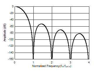
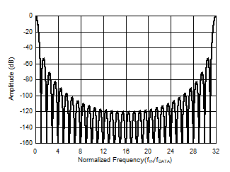
Figure 7-18 and Figure 7-19 show the sinc4 filter frequency response at OSR = 32. The frequency response consists of a series of response nulls occurring at discrete frequencies. These null frequencies occur at multiples of fDATA. At the null frequencies, the filter has zero gain. A folded image of the overall frequency response appears at multiples of fMOD, as illustrated in the frequency plot of Figure 7-19. Attenuation is not provided by the filter at input frequencies near n × fMOD (n = 1, 2, 3, and so on). If present at these frequencies, aliases occurs in the pass band.
 Figure 7-18 Sinc4 Frequency
Response
Figure 7-18 Sinc4 Frequency
Response(OSR = 32)
 Figure 7-19 Sinc4 Frequency Response
to fMOD (OSR = 32)