SLUSC86D March   2015  – October 2022 BQ25890 , BQ25892

PRODUCTION DATA  

  1. Features
  2. Applications
  3. Description
  4. Revision History
  5. Description (continued)
  6. Device Comparison Table
  7. Pin Configuration and Functions
  8. Specifications
    1. 8.1 Absolute Maximum Ratings (1)
    2. 8.2 ESD Ratings
    3. 8.3 Recommended Operating Conditions
    4. 8.4 Thermal Information
    5. 8.5 Electrical Characteristics
    6. 8.6 Timing Requirements
    7. 8.7 Typical Characteristics
  9. Detailed Description
    1. 9.1 Functional Block Diagram
    2. 9.2 Feature Description
      1. 9.2.1  Device Power-On-Reset (POR)
      2. 9.2.2  Device Power Up from Battery without Input Source
      3. 9.2.3  Device Power Up from Input Source
        1. 9.2.3.1 Power Up REGN Regulation (LDO)
        2. 9.2.3.2 Poor Source Qualification
        3. 9.2.3.3 Input Source Type Detection
          1. 9.2.3.3.1 D+/D– Detection Sets Input Current Limit (BQ25890)
          2. 9.2.3.3.2 PSEL/OTG Pins Set Input Current Limit (BQ25892)
          3. 9.2.3.3.3 Force Input Current Limit Detection
        4. 9.2.3.4 Input Voltage Limit Threshold Setting (VINDPM Threshold)
        5. 9.2.3.5 Converter Power-Up
      4. 9.2.4  Input Current Optimizer (ICO)
      5. 9.2.5  Boost Mode Operation from Battery
      6. 9.2.6  Power Path Management
        1. 9.2.6.1 Narrow VDC Architecture
        2. 9.2.6.2 Dynamic Power Management
        3. 9.2.6.3 Supplement Mode
      7. 9.2.7  Battery Charging Management
        1. 9.2.7.1 Autonomous Charging Cycle
        2. 9.2.7.2 Battery Charging Profile
        3. 9.2.7.3 Charging Termination
        4. 9.2.7.4 Resistance Compensation (IRCOMP)
        5. 9.2.7.5 Thermistor Qualification
          1. 9.2.7.5.1 JEITA Guideline Compliance in Charge Mode
          2. 9.2.7.5.2 Cold/Hot Temperature Window in Boost Mode
        6. 9.2.7.6 Charging Safety Timer
      8. 9.2.8  Battery Monitor
      9. 9.2.9  Status Outputs ( PG, STAT, and INT)
        1. 9.2.9.1 Power Good Indicator ( PG)
        2. 9.2.9.2 Charging Status Indicator (STAT)
        3. 9.2.9.3 Interrupt to Host (INT)
      10. 9.2.10 BATET (Q4) Control
        1. 9.2.10.1 BATFET Disable Mode (Shipping Mode)
        2. 9.2.10.2 BATFET Enable (Exit Shipping Mode)
        3. 9.2.10.3 BATFET Full System Reset
      11. 9.2.11 Current Pulse Control Protocol
      12. 9.2.12 Input Current Limit on ILIM
      13. 9.2.13 Thermal Regulation and Thermal Shutdown
        1. 9.2.13.1 Thermal Protection in Buck Mode
        2. 9.2.13.2 Thermal Protection in Boost Mode
      14. 9.2.14 Voltage and Current Monitoring in Buck and Boost Mode
        1. 9.2.14.1 Voltage and Current Monitoring in Buck Mode
          1. 9.2.14.1.1 Input Overvoltage (ACOV)
          2. 9.2.14.1.2 System Overvoltage Protection (SYSOVP)
        2. 9.2.14.2 Voltage and Current Monitoring in Boost Mode
          1. 9.2.14.2.1 VBUS Overcurrent Protection
          2. 9.2.14.2.2 Boost Mode Overvoltage Protection
      15. 9.2.15 Battery Protection
        1. 9.2.15.1 Battery Overvoltage Protection (BATOVP)
        2. 9.2.15.2 Battery Over-Discharge Protection
        3. 9.2.15.3 System Overcurrent Protection
      16. 9.2.16 Serial Interface
        1. 9.2.16.1 Data Validity
        2. 9.2.16.2 START and STOP Conditions
        3. 9.2.16.3 Byte Format
        4. 9.2.16.4 Acknowledge (ACK) and Not Acknowledge (NACK)
        5. 9.2.16.5 Target Address and Data Direction Bit
        6. 9.2.16.6 Single Read and Write
        7. 9.2.16.7 Multi-Read and Multi-Write
    3. 9.3 Device Functional Modes
      1. 9.3.1 Host Mode and Default Mode
    4. 9.4 Register Maps
      1. 9.4.1  REG00
      2. 9.4.2  REG01
      3. 9.4.3  REG02
      4. 9.4.4  REG03
      5. 9.4.5  REG04
      6. 9.4.6  REG05
      7. 9.4.7  REG06
      8. 9.4.8  REG07
      9. 9.4.9  REG08
      10. 9.4.10 REG09
      11. 9.4.11 REG0A
      12. 9.4.12 REG0B
      13. 9.4.13 REG0C
      14. 9.4.14 REG0D
      15. 9.4.15 REG0E
      16. 9.4.16 REG0F
      17. 9.4.17 REG10
      18. 9.4.18 REG11
      19. 9.4.19 REG12
      20. 9.4.20 REG13
      21. 9.4.21 REG14
  10. 10Application and Implementation
    1. 10.1 Application Information
    2. 10.2 Typical Application
      1. 10.2.1 Design Requirements
      2. 10.2.2 Detailed Design Procedure
        1. 10.2.2.1 Inductor Selection
        2. 10.2.2.2 Buck Input Capacitor
        3. 10.2.2.3 System Output Capacitor
      3. 10.2.3 Application Curves
    3. 10.3 System Examples
  11. 11Power Supply Recommendations
  12. 12Layout
    1. 12.1 Layout Guidelines
    2. 12.2 Layout Example
  13. 13Device and Documentation Support
    1. 13.1 Device Support
      1. 13.1.1 Third-Party Products Disclaimer
    2. 13.2 Receiving Notification of Documentation Updates
    3. 13.3 Support Resources
    4. 13.4 Trademarks
    5. 13.5 Electrostatic Discharge Caution
    6. 13.6 Glossary
  14. 14Mechanical, Packaging, and Orderable Information

Package Options

Mechanical Data (Package|Pins)
Thermal pad, mechanical data (Package|Pins)
Orderable Information
JEITA Guideline Compliance in Charge Mode

To improve the safety of charging Li-ion batteries, JEITA guideline was released on April 20, 2007. The guideline emphasized the importance of avoiding a high charge current and high charge voltage at certain low and high temperature ranges.

The device continuously monitors battery temperature by measuring the voltage between the TS pins and ground, typically determined by a negative temperature coefficient thermistor (NTC) and an external voltage divider. The device compares this voltage against its internal thresholds to determine if charging is allowed. To initiate a charge cycle, the voltage on TS pin must be within the VT1 to VT5 thresholds. If TS voltage exceeds the T1–T5 range, the controller suspends charging and waits until the battery temperature is within the T1 to T5 range. At cool temperature (T1–T2), JEITA recommends the charge current to be reduced to at least half of the charge current or lower. At warm temperature (T3–T5), JEITA recommends charge voltage below nominal charge voltage.

The device provides flexible voltage/current settings beyond the JEITA requirement. The voltage setting at warm temperature (T3–T5) can be 200 mV below charge voltage (JEITA_VSET=0). The current setting at cool temperature (T1–T2) can be further reduced to 20% or 50% of fast charge current (JEITA_ISET bit).

GUID-8B6D27D7-F096-419D-B03A-8B6EF909930F-low.gifFigure 9-6 TS Resistor Network
GUID-E469528B-6BCE-46F2-92CA-515EC19972B6-low.gifFigure 9-7 Charging Values

Assuming a 103AT NTC thermistor on the battery pack as shown in Figure 9-6, the value RT1 and RT2 can be determined by using Equation 2:

Equation 2. GUID-B7272714-4752-4F7C-8138-49D60E88F8FF-low.gif

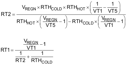
Select 0°C to 60°C range for Li-ion or Li-polymer battery,
RTHT1 = 27.28 kΩ
RTHT5 = 3.02 kΩ
RT1 = 5.24 kΩ
RT2 = 30.31 kΩ