SNLS603D December   2020  – April 2025 DP83TG720R-Q1

PRODUCTION DATA  

  1.   1
  2. Features
  3. Applications
  4. Description
  5. Device Comparison Table
  6. Pin Configuration and Functions
    1.     Pin Functions
    2. 5.1 Pin States
    3. 5.2 Pin Power Domain
  7. Specifications
    1. 6.1 Absolute Maximum Ratings
    2. 6.2 ESD Ratings
    3. 6.3 Recommended Operating Conditions
    4. 6.4 Thermal Information
    5. 6.5 Electrical Characteristics
    6. 6.6 Timing Requirements
    7. 6.7 Timing Diagrams
    8. 6.8 LED Drive Characteristics
  8. Detailed Description
    1. 7.1 Overview
    2. 7.2 Functional Block Diagram
    3. 7.3 Feature Description
      1. 7.3.1 Diagnostic Tool Kit
        1. 7.3.1.1 Signal Quality Indicator
        2. 7.3.1.2 Time Domain Reflectometry
        3. 7.3.1.3 Built-In Self-Test For Datapath
          1. 7.3.1.3.1 Loopback Modes
          2. 7.3.1.3.2 Data Generator
          3. 7.3.1.3.3 Programming Datapath BIST
        4. 7.3.1.4 Temperature and Voltage Sensing
        5. 7.3.1.5 Electrostatic Discharge Sensing
      2. 7.3.2 Compliance Test Modes
        1. 7.3.2.1 Test Mode 1
        2. 7.3.2.2 Test Mode 2
        3. 7.3.2.3 Test Mode 4
        4. 7.3.2.4 Test Mode 5
        5. 7.3.2.5 Test Mode 6
        6. 7.3.2.6 Test Mode 7
    4. 7.4 Device Functional Modes
      1. 7.4.1 Power Down
      2. 7.4.2 Reset
      3. 7.4.3 Standby
      4. 7.4.4 Normal
      5. 7.4.5 Sleep
      6. 7.4.6 State Transitions
        1. 7.4.6.1 State Transition #1 - Standby to Normal
        2. 7.4.6.2 State Transition #2 - Normal to Standby
        3. 7.4.6.3 State Transition #3 - Normal to Sleep
        4. 7.4.6.4 State Transition #4 - Sleep to Normal
      7. 7.4.7 Media Dependent Interface
        1. 7.4.7.1 MDI Master and MDI Slave Configuration
        2. 7.4.7.2 Auto-Polarity Detection and Correction
      8. 7.4.8 MAC Interfaces
        1. 7.4.8.1 Reduced Gigabit Media Independent Interface
      9. 7.4.9 Serial Management Interface
        1. 7.4.9.1 Direct Register Access
        2. 7.4.9.2 Extended Register Space Access
          1. 7.4.9.2.1 Write Operation (No Post Increment)
          2. 7.4.9.2.2 Read Operation (No Post Increment)
          3. 7.4.9.2.3 Write Operation (Post Increment)
          4. 7.4.9.2.4 Read Operation (Post Increment)
    5. 7.5 Programming
      1. 7.5.1 Strap Configuration
      2. 7.5.2 LED Configuration
      3. 7.5.3 PHY Address Configuration
    6. 7.6 Register Maps
      1. 7.6.1 Register Access Summary
      2. 7.6.2 DP83TG720 Registers
  9. Application and Implementation
    1. 8.1 Application Information
    2. 8.2 Typical Applications
      1. 8.2.1 Design Requirements
    3. 8.3 Power Supply Recommendations
    4. 8.4 Compatibility with TI's 100BT1 PHY
    5. 8.5 Layout
      1. 8.5.1 Layout Guidelines
        1. 8.5.1.1 Signal Traces
        2. 8.5.1.2 Return Path
        3. 8.5.1.3 Physical Medium Attachment
        4. 8.5.1.4 Metal Pour
        5. 8.5.1.5 PCB Layer Stacking
  10. Device and Documentation Support
    1. 9.1 Receiving Notification of Documentation Updates
    2. 9.2 Support Resources
    3. 9.3 Trademarks
    4. 9.4 Electrostatic Discharge Caution
    5. 9.5 Glossary
  11. 10Revision History
  12. 11Mechanical, Packaging, and Orderable Information
    1. 11.1 Package Option Addendum
      1. 11.1.1 Packaging Information
      2. 11.1.2 Tape and Reel Information

Package Options

Mechanical Data (Package|Pins)
Thermal pad, mechanical data (Package|Pins)
Orderable Information

Sleep

Once in sleep mode, all PHY blocks are disabled except for energy detection. All register configurations are lost in sleep mode. No link can be established, data cannot be transmitted or received and SMI access is not available when in sleep mode.

To use sleep mode of PHY refer to implementation highlighted in following figure.
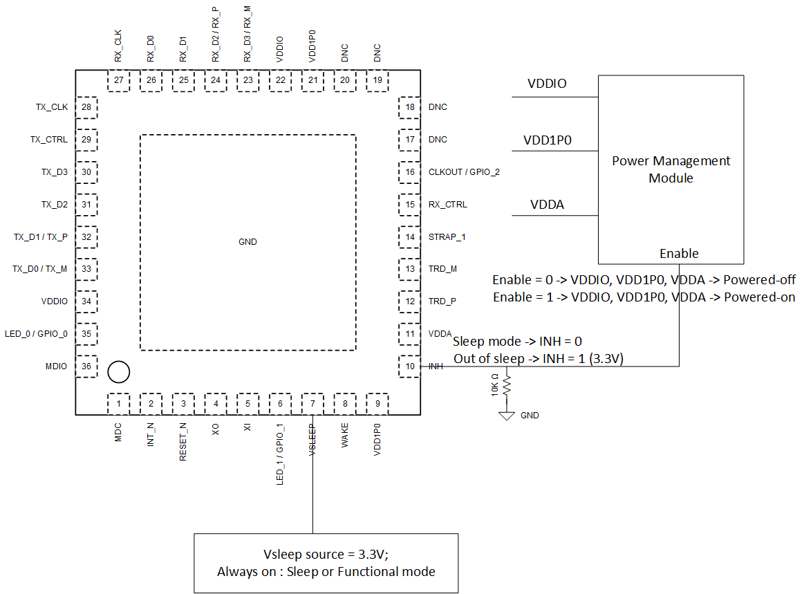
DP83TG720R-Q1 Required Implementation for Sleep
          Mode Figure 7-12 Required Implementation for Sleep Mode
Note: Phy does not go into sleep mode if supply sources are not disabled as per above figure.