SNLS603D December   2020  – April 2025 DP83TG720R-Q1

PRODUCTION DATA  

  1.   1
  2. Features
  3. Applications
  4. Description
  5. Device Comparison Table
  6. Pin Configuration and Functions
    1.     Pin Functions
    2. 5.1 Pin States
    3. 5.2 Pin Power Domain
  7. Specifications
    1. 6.1 Absolute Maximum Ratings
    2. 6.2 ESD Ratings
    3. 6.3 Recommended Operating Conditions
    4. 6.4 Thermal Information
    5. 6.5 Electrical Characteristics
    6. 6.6 Timing Requirements
    7. 6.7 Timing Diagrams
    8. 6.8 LED Drive Characteristics
  8. Detailed Description
    1. 7.1 Overview
    2. 7.2 Functional Block Diagram
    3. 7.3 Feature Description
      1. 7.3.1 Diagnostic Tool Kit
        1. 7.3.1.1 Signal Quality Indicator
        2. 7.3.1.2 Time Domain Reflectometry
        3. 7.3.1.3 Built-In Self-Test For Datapath
          1. 7.3.1.3.1 Loopback Modes
          2. 7.3.1.3.2 Data Generator
          3. 7.3.1.3.3 Programming Datapath BIST
        4. 7.3.1.4 Temperature and Voltage Sensing
        5. 7.3.1.5 Electrostatic Discharge Sensing
      2. 7.3.2 Compliance Test Modes
        1. 7.3.2.1 Test Mode 1
        2. 7.3.2.2 Test Mode 2
        3. 7.3.2.3 Test Mode 4
        4. 7.3.2.4 Test Mode 5
        5. 7.3.2.5 Test Mode 6
        6. 7.3.2.6 Test Mode 7
    4. 7.4 Device Functional Modes
      1. 7.4.1 Power Down
      2. 7.4.2 Reset
      3. 7.4.3 Standby
      4. 7.4.4 Normal
      5. 7.4.5 Sleep
      6. 7.4.6 State Transitions
        1. 7.4.6.1 State Transition #1 - Standby to Normal
        2. 7.4.6.2 State Transition #2 - Normal to Standby
        3. 7.4.6.3 State Transition #3 - Normal to Sleep
        4. 7.4.6.4 State Transition #4 - Sleep to Normal
      7. 7.4.7 Media Dependent Interface
        1. 7.4.7.1 MDI Master and MDI Slave Configuration
        2. 7.4.7.2 Auto-Polarity Detection and Correction
      8. 7.4.8 MAC Interfaces
        1. 7.4.8.1 Reduced Gigabit Media Independent Interface
      9. 7.4.9 Serial Management Interface
        1. 7.4.9.1 Direct Register Access
        2. 7.4.9.2 Extended Register Space Access
          1. 7.4.9.2.1 Write Operation (No Post Increment)
          2. 7.4.9.2.2 Read Operation (No Post Increment)
          3. 7.4.9.2.3 Write Operation (Post Increment)
          4. 7.4.9.2.4 Read Operation (Post Increment)
    5. 7.5 Programming
      1. 7.5.1 Strap Configuration
      2. 7.5.2 LED Configuration
      3. 7.5.3 PHY Address Configuration
    6. 7.6 Register Maps
      1. 7.6.1 Register Access Summary
      2. 7.6.2 DP83TG720 Registers
  9. Application and Implementation
    1. 8.1 Application Information
    2. 8.2 Typical Applications
      1. 8.2.1 Design Requirements
    3. 8.3 Power Supply Recommendations
    4. 8.4 Compatibility with TI's 100BT1 PHY
    5. 8.5 Layout
      1. 8.5.1 Layout Guidelines
        1. 8.5.1.1 Signal Traces
        2. 8.5.1.2 Return Path
        3. 8.5.1.3 Physical Medium Attachment
        4. 8.5.1.4 Metal Pour
        5. 8.5.1.5 PCB Layer Stacking
  10. Device and Documentation Support
    1. 9.1 Receiving Notification of Documentation Updates
    2. 9.2 Support Resources
    3. 9.3 Trademarks
    4. 9.4 Electrostatic Discharge Caution
    5. 9.5 Glossary
  11. 10Revision History
  12. 11Mechanical, Packaging, and Orderable Information
    1. 11.1 Package Option Addendum
      1. 11.1.1 Packaging Information
      2. 11.1.2 Tape and Reel Information

Package Options

Mechanical Data (Package|Pins)
Thermal pad, mechanical data (Package|Pins)
Orderable Information

Typical Applications

DP83TG720R-Q1 Typical
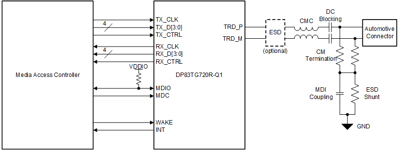
                    Application (RGMII) Figure 8-1 Typical Application (RGMII)
Table 8-1 Recommended Components for MDI Network
Design Parameter Value
DC Blocking Capacitors 1 0.1μF
Common-Mode Choke

Murata :DLW32MH101XT2

Common Mode Termination Resistors 12 1kΩ
MDI Coupling Capacitor 4.7nF
ESD Shunt 100kΩ
  1. 1% tolerance components are recommended for margins over spec of return loss and mode conversion.
  2. CM termination resistor's size higher than 0805 helps in increasing ESD margin.