SNLS603C December   2020  – November 2022 DP83TG720R-Q1

PRODUCTION DATA  

  1. Features
  2. Applications
  3. Description
  4. Revision History
  5. Device Comparison Table
  6. Pin Configuration and Functions
    1.     Pin Functions
    2. 6.1 Pin States
    3. 6.2 Pin Power Domain
  7. Specifications
    1. 7.1 Absolute Maximum Ratings
    2. 7.2 ESD Ratings
    3. 7.3 Recommended Operating Conditions
    4. 7.4 Thermal Information
    5. 7.5 Electrical Characteristics
    6. 7.6 Timing Requirements
    7. 7.7 Timing Diagrams
    8. 7.8 LED Drive Characteristics
  8. Detailed Description
    1. 8.1 Overview
    2. 8.2 Functional Block Diagram
    3. 8.3 Feature Description
      1. 8.3.1 Diagnostic Tool Kit
        1. 8.3.1.1 Signal Quality Indicator
        2. 8.3.1.2 Time Domain Reflectometry
        3. 8.3.1.3 Built-In Self-Test For Datapath
          1. 8.3.1.3.1 Loopback Modes
          2. 8.3.1.3.2 Data Generator
          3. 8.3.1.3.3 Programming Datapath BIST
        4. 8.3.1.4 Temperature and Voltage Sensing
        5. 8.3.1.5 Electrostatic Discharge Sensing
      2. 8.3.2 Compliance Test Modes
        1. 8.3.2.1 Test Mode 1
        2. 8.3.2.2 Test Mode 2
        3. 8.3.2.3 Test Mode 4
        4. 8.3.2.4 Test Mode 5
        5. 8.3.2.5 Test Mode 6
        6. 8.3.2.6 Test Mode 7
    4. 8.4 Device Functional Modes
      1. 8.4.1  Power Down
      2. 8.4.2  Reset
      3. 8.4.3  Standby
      4. 8.4.4  Normal
      5. 8.4.5  Sleep
      6. 8.4.6  State Transitions
        1. 8.4.6.1 State Transition #1 - Standby to Normal
        2. 8.4.6.2 State Transition #2 - Normal to Standby
        3. 8.4.6.3 State Transition #3 - Normal to Sleep
        4. 8.4.6.4 State Transition #4 - Sleep to Normal
      7. 8.4.7  Media Dependent Interface
        1. 8.4.7.1 MDI Master and MDI Slave Configuration
        2. 8.4.7.2 Auto-Polarity Detection and Correction
      8. 8.4.8  MAC Interfaces
        1. 8.4.8.1 Reduced Gigabit Media Independent Interface
      9. 8.4.9  Serial Management Interface
      10. 8.4.10 Direct Register Access
      11. 8.4.11 Extended Register Space Access
      12. 8.4.12 Write Address Operation
        1. 8.4.12.1 Example - Write Address Operation
      13. 8.4.13 Read Address Operation
        1. 8.4.13.1 Example - Read Address Operation
      14. 8.4.14 Write Operation (No Post Increment)
        1. 8.4.14.1 Example - Write Operation (No Post Increment)
      15. 8.4.15 Read Operation (No Post Increment)
        1. 8.4.15.1 Example - Read Operation (No Post Increment)
      16. 8.4.16 Write Operation (Post Increment)
        1. 8.4.16.1 Example - Write Operation (Post Increment)
      17. 8.4.17 Read Operation (Post Increment)
        1. 8.4.17.1 Example - Read Operation (Post Increment)
    5. 8.5 Programming
      1. 8.5.1 Strap Configuration
      2. 8.5.2 LED Configuration
      3. 8.5.3 PHY Address Configuration
    6. 8.6 Register Maps
      1. 8.6.1 Register Access Summary
      2. 8.6.2 DP83TG720 Registers
        1. 8.6.2.1 Base Registers
  9. Application and Implementation
    1. 9.1 Application Information
    2. 9.2 Typical Applications
      1. 9.2.1 Design Requirements
  10. 10Power Supply Recommendations
  11. 11Compatibility with TI's 100BT1 PHY
  12. 12Layout
    1. 12.1 Layout Guidelines
      1. 12.1.1 Signal Traces
      2. 12.1.2 Return Path
      3. 12.1.3 Physical Medium Attachment
      4. 12.1.4 Metal Pour
      5. 12.1.5 PCB Layer Stacking
  13. 13Device and Documentation Support
    1. 13.1 Receiving Notification of Documentation Updates
    2. 13.2 Support Resources
    3. 13.3 Trademarks
    4. 13.4 Electrostatic Discharge Caution
    5. 13.5 Glossary
  14. 14Mechanical, Packaging, and Orderable Information
    1. 14.1 Package Option Addendum
      1. 14.1.1 Packaging Information
      2. 14.1.2 Tape and Reel Information

Package Options

Mechanical Data (Package|Pins)
Thermal pad, mechanical data (Package|Pins)
Orderable Information

Power Supply Recommendations

The DP83TG720R-Q1 is capable of operating with a wide range of IO supply voltages (3.3 V, 2.5 V, or 1.8 V). No power supply sequencing is required. The recommended power supply de-coupling network is shown in following figure :
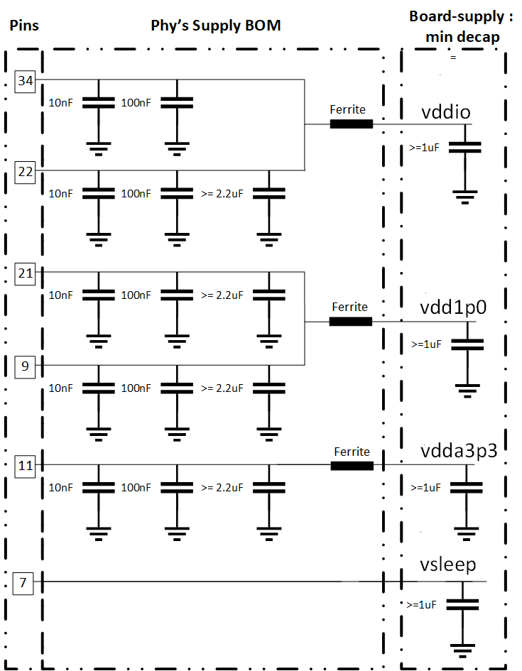
GUID-B85A6067-9235-43AA-9A40-8F2838079AE8-low.gif Figure 10-1 Recommended Supply De-Coupling Network (if sleep mode is used in the application)
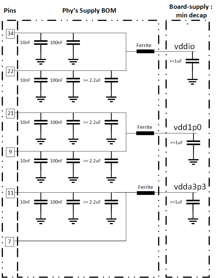
GUID-E868E084-0A85-4899-AB08-F70B0D26700F-low.gif Figure 10-2 Recommended Supply De-Coupling Network (if sleep mode is not used in application)

Table 10-1 Recommended Components for Power Network
Design Parameter Value
VDDIO 1.8 V, 2.5 V, or 3.3 V
De-Coupling Capacitors VDDIO (pin 34) 10 nF, 100 nF
De-Coupling Capacitors VDDIO (pin 22) 10 nF, 100 nF, 2.2uF
Combined Ferrite Bead for VDDIO BLM18HE102SN1
VDDA 3.3 V
De-Coupling Capacitors VDDA (pin 11) 10 nF, 100 nF, 2.2uF
Ferrite Bead for VDDA BLM18KG601SH1
VDD1p0 1 V
De-Coupling Capacitors VDD1P0 (pin 9) 10 nF, 100 nF, 2.2uF
De-Coupling Capacitors VDDA (pin 21) 10 nF, 100 nF, 2.2uF
Combined Ferrite Bead for VDD1P0 BLM18KG601SH1
Vsleep 3.3 V

Note: For recommendation on LDOs for VDD1p0 and Vsleep, please refer to the DP83TC811, DP83TG730 Rollover Document application report.