SLVSI22 August 2025 DRV8844A
PRODUCTION DATA
- 1
- 1 Features
- 2 Applications
- 3 Description
- 4 Pin Configuration and Functions
- 5 Specifications
- 6 Detailed Description
- 7 Application and Implementation
- 8 Device and Documentation Support
- 9 Revision History
- 10Mechanical, Packaging, and Orderable Information
Package Options
Mechanical Data (Package|Pins)
- DGQ|28
Thermal pad, mechanical data (Package|Pins)
- DGQ|28
Orderable Information
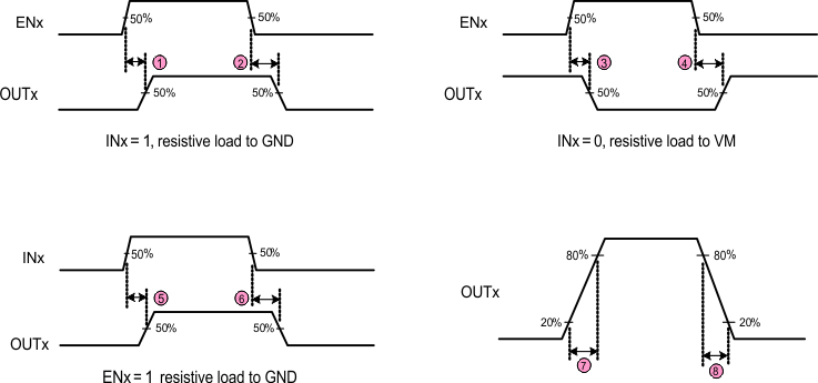
5.6 Switching Characteristics
over operating free-air temperature range (unless otherwise noted)(1) (see Figure 5-1)
| NUMBER | PARAMETER | TEST CONDITIONS | MIN | MAX | UNIT |
|---|---|---|---|---|---|
| 1 | t1 | Delay time, ENx high to OUTx high, INx = 1 | 130 | 330 | ns |
| 2 | t2 | Delay time, ENx low to OUTx low, INx = 1 | 275 | 475 | ns |
| 3 | t3 | Delay time, ENx high to OUTx low, INx = 0 | 100 | 300 | ns |
| 4 | t4 | Delay time, ENx low to OUTx high, INx = 0 | 200 | 400 | ns |
| 5 | t5 | Delay time, INx high to OUTx high | 300 | 500 | ns |
| 6 | t6 | Delay time, INx low to OUTx low | 275 | 475 | ns |
| 7 | tR | Output rise time, resistive load to VNEG | 30 | 150 | ns |
| 8 | tF | Output fall time, resistive load to VNEG | 30 | 150 | ns |
(1) Not production tested
 Figure 5-1 DRV8844A Switching Characteristics