SLVSI22 August 2025 DRV8844A
PRODUCTION DATA
- 1
- 1 Features
- 2 Applications
- 3 Description
- 4 Pin Configuration and Functions
- 5 Specifications
- 6 Detailed Description
- 7 Application and Implementation
- 8 Device and Documentation Support
- 9 Revision History
- 10Mechanical, Packaging, and Orderable Information
Package Options
Mechanical Data (Package|Pins)
- DGQ|28
Thermal pad, mechanical data (Package|Pins)
- DGQ|28
Orderable Information
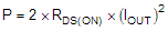
7.4.4 Power Dissipation
Power dissipation in the DRV8844A is dominated by the power dissipated in the output FET resistance, or RDS(ON). Average power dissipation of each H-bridge when running a DC motor can be roughly estimated by Equation 5.
where
- P is the power dissipation of one H-bridge
- RDS(ON) is the resistance of each FET
- IOUT is the RMS output current being applied to each winding
IOUT is equal to the average current drawn by the DC motor. Note that at start-up and fault conditions this current is much higher than normal running current; these peak currents and the duration also need to be taken into consideration. The factor of 2 comes from the fact that at any instant two FETs are conducting winding current (one high-side and one low-side).
The total device dissipation is the power dissipated in each of the two H-bridges added together.
The maximum amount of power that can be dissipated in the device is dependent on ambient temperature and heatsinking.
Note that RDS(ON) increases with temperature, so as the device heats, the power dissipation increases. This must be taken into consideration when sizing the heatsink.