SNVSB29C October 2018 – June 2021 LM5143-Q1
PRODUCTION DATA
- 1 Features
- 2 Applications
- 3 Description
- 4 Revision History
- 5 Description (continued)
- 6 Pin Configuration and Functions
- 7 Specifications
-
8 Detailed Description
- 8.1 Overview
- 8.2 Functional Block Diagram
- 8.3
Feature Description
- 8.3.1 Input Voltage Range (VIN)
- 8.3.2 High-Voltage Bias Supply Regulator (VCC, VCCX, VDDA)
- 8.3.3 Enable (EN1, EN2)
- 8.3.4 Power Good Monitor (PG1, PG2)
- 8.3.5 Switching Frequency (RT)
- 8.3.6 Clock Synchronization (DEMB)
- 8.3.7 Synchronization Out (SYNCOUT)
- 8.3.8 Spread Spectrum Frequency Modulation (DITH)
- 8.3.9 Configurable Soft Start (SS1, SS2)
- 8.3.10 Output Voltage Setpoint (FB1, FB2)
- 8.3.11 Minimum Controllable On-Time
- 8.3.12 Error Amplifier and PWM Comparator (FB1, FB2, COMP1, COMP2)
- 8.3.13 Slope Compensation
- 8.3.14 Inductor Current Sense (CS1, VOUT1, CS2, VOUT2)
- 8.3.15 Hiccup Mode Current Limiting (RES)
- 8.3.16 High-Side and Low-Side Gate Drivers (HO1/2, LO1/2, HOL1/2, LOL1/2)
- 8.3.17 Output Configurations (MODE, FB2)
- 8.4 Device Functional Modes
-
9 Application and Implementation
- 9.1 Application Information
- 9.2 Typical Applications
- 10Power Supply Recommendations
- 11Layout
- 12Device and Documentation Support
- 13Mechanical, Packaging, and Orderable Information
Package Options
Mechanical Data (Package|Pins)
- RWG|40
Thermal pad, mechanical data (Package|Pins)
Orderable Information
8.3.9 Configurable Soft Start (SS1, SS2)
The soft-start feature allows the regulator to gradually reach the steady-state operating point, thus reducing start-up stresses and surges.
The LM5143-Q1 features an adjustable soft start that determines the charging time of the output or outputs. Soft start limits inrush current as a result of high output capacitance to avoid an overcurrent condition. Stress on the input supply rail is also reduced.
The LM5143-Q1 regulates the FB voltage to the SS voltage or the internal 600-mV reference, whichever is lower. At the beginning of the soft-start sequence when the SS voltage is 0 V, the internal 21-μA soft-start current source gradually increases the voltage on an external soft-start capacitor connected to the SS pin, resulting in a gradual rise of the relevant FB and output voltages. Use Equation 4 to calculate the soft-start capacitance.
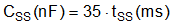
where
- tSS is the required soft-start time
SS can be pulled low with an external circuit to stop switching, but this is not recommended. When the controller is in FPWM mode (set by connecting DEMB to VDDA), pulling SS low results in COMP being pulled down internally as well. LO remains on and the low-side MOSFET discharges the output capacitor, resulting in large negative inductor current. In contrast, the LO gate driver is disabled when the LM5143-Q1 internal logic pulls SS low due to a fault condition.