SNIS133E September 2003 – February 2024 LM95010
PRODUCTION DATA
- 1
- 1 Features
- 2 Applications
- 3 Description
- 4 Pin Configuration and Functions
- 5 Specifications
-
6 Detailed Description
- 6.1 Overview
- 6.2 Functional Block Diagram
- 6.3
Feature Description
- 6.3.1 SensorPath BUS SWD
- 6.3.2 SensorPath BIT SIGNALING
- 6.3.3 Bus Inactive
- 6.3.4 Data Bit 0 and 1
- 6.3.5 Start Bit
- 6.3.6 Attention Request
- 6.3.7 Bus Reset
- 6.3.8 SensorPath BUS TRANSACTIONS
- 6.3.9 Bus Reset Operation
- 6.3.10 Read Transaction
- 6.3.11 Write Transaction
- 6.3.12 Read and Write Transaction Exceptions
- 6.3.13 Attention Request Transaction
-
7 Register Set
- 7.1 Fixed Number Setting
- 7.2 Register Set Summary
- 7.3 Device Reset Operation
- 7.4 Device Number (Addr 00o)
- 7.5 Manufacturer ID (Addr 01o)
- 7.6 Device ID (Addr 02o)
- 7.7 Capabilities Fixed (Addr 03o)
- 7.8 Device Status (Addr 04o)
- 7.9 Device Control (Addr 05o)
- 7.10 Temperature Measurement Function (TYPE - 0001)
- 7.11 Operation
- 7.12 Temperature Capabilities (Addr 10o)
- 7.13 Temperature Data Readout (Addr 11o)
- 7.14 Temperature Control (Addr 12o)
- 7.15 Conversion Rate (Addr 40o)
- 8 Application and Implementation
- 9 Device and Documentation Support
- 10Revision History
- 11Mechanical, Packaging, and Orderable Information
Package Options
Mechanical Data (Package|Pins)
- DGK|8
Thermal pad, mechanical data (Package|Pins)
Orderable Information
4 Pin Configuration and Functions
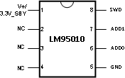
 Figure 4-1 8-Lead
VSSOP See DGK Package
Figure 4-1 8-Lead
VSSOP See DGK PackageTable 4-1 Pin Descriptions
| Pin Number | Pin Name | Type | Description | Typical Connection |
|---|---|---|---|---|
| 1 | V+/3.3V SB | Power | Positive power supply pin +3.3V pin. | Should be powered by +3.3V Standby power. This pin should be bypassed with a 0.1 µF capacitor. A bulk capacitance of approximately 10 µF needs to be in the near vicinity of the LM95010. |
| 2-4 | NC | Must be grounded. | ||
| 5 | GND | Power | Ground | System ground |
| 6 | ADD0 | Input | Address select input that assigns the serial bus device number | 10kΩ resistor to V+ or GND; must never be left floating |
| 7 | ADD1 | Input | Address select input that assigns the serial bus device number | 10kΩ resistor to V+ or GND; must never be left floating |
| 8 | SWD | Input/ Output | Single-wire Data, SensorPath serial interface line; Open-drain output | Super I/O with 1.25kΩ pull-up to 3.3V |