SNAS918 May 2025 LMK5C23208A
PRODUCTION DATA
- 1
- 1 Features
- 2 Applications
- 3 Description
- 4 Device Comparison
- 5 Pin Configuration and Functions
- 6 Specifications
- 7 Parameter Measurement Information
-
8 Detailed Description
- 8.1 Overview
- 8.2 Functional Block Diagram
- 8.3
Feature Description
- 8.3.1 Oscillator Input (XO)
- 8.3.2 Reference Inputs
- 8.3.3 Clock Input Interfacing and Termination
- 8.3.4 Reference Input Mux Selection
- 8.3.5 Hitless Switching
- 8.3.6 Gapped Clock Support on Reference Inputs
- 8.3.7 Input Clock and PLL Monitoring, Status, and Interrupts
- 8.3.8
PLL Relationships
- 8.3.8.1 PLL Frequency Relationships
- 8.3.8.2 Analog PLLs (APLL1, APLL2)
- 8.3.8.3 APLL Reference Paths
- 8.3.8.4 APLL Feedback Divider Paths
- 8.3.8.5 APLL Loop Filters (LF1, LF2)
- 8.3.8.6 APLL Voltage-Controlled Oscillators (VCO1, VCO2)
- 8.3.8.7 APLL VCO Clock Distribution Paths
- 8.3.8.8 DPLL Reference (R) Divider Paths
- 8.3.8.9 DPLL Time-to-Digital Converter (TDC)
- 8.3.8.10 DPLL Loop Filter (DLF)
- 8.3.8.11 DPLL Feedback (FB) Divider Path
- 8.3.9 Output Clock Distribution
- 8.3.10 Output Source Muxes
- 8.3.11 Output Channel Muxes
- 8.3.12 Output Dividers (OD)
- 8.3.13 SYSREF/1PPS Output
- 8.3.14 Output Delay
- 8.3.15 Clock Output Drivers
- 8.3.16 Clock Output Interfacing and Termination
- 8.3.17 Glitchless Output Clock Start-Up
- 8.3.18 Output Auto-Mute During LOL
- 8.3.19 Output Synchronization (SYNC)
- 8.3.20 Zero-Delay Mode (ZDM)
- 8.3.21 DPLL Programmable Phase Delay
- 8.3.22 Time Elapsed Counter (TEC)
- 8.4 Device Functional Modes
- 8.5 Programming
-
9 Application and Implementation
- 9.1 Application Information
- 9.2 Typical Application
- 9.3 Best Design Practices
- 9.4 Power Supply Recommendations
- 9.5 Layout
- 10Device and Documentation Support
- 11Revision History
- 12Mechanical, Packaging, and Orderable Information
Package Options
Mechanical Data (Package|Pins)
- RGC|64
Thermal pad, mechanical data (Package|Pins)
- RGC|64
Orderable Information
9.5.2 Layout Example
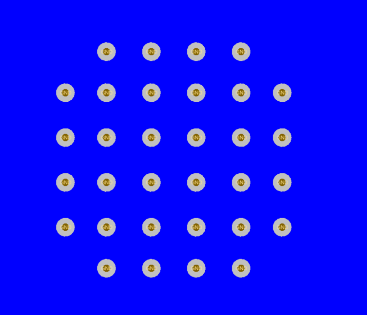
Below are printed circuit board (PCB) layout examples that show the application of thermal design practices and a low-inductance ground connection between the device DAP and the PCB. Place the ground return path for the supply decoupling capacitors close to the DAP. All OUTx pairs configured as differential signals must be routed differentially and meet the trace impedance requirements (typically 100 ohm differential).
Figure 9-5 PCB Layout Example for LMK5C23208A, Top
Layer
 Figure 9-6 PCB Layout Example for LMK5C23208A, Bottom Layer