SNAS918 May   2025 LMK5C23208A

PRODUCTION DATA  

  1.   1
  2. Features
  3. Applications
  4. Description
  5. Device Comparison
  6. Pin Configuration and Functions
  7. Specifications
    1. 6.1 Absolute Maximum Ratings
    2. 6.2 ESD Ratings
    3. 6.3 Recommended Operating Conditions
    4. 6.4 Thermal Information
    5. 6.5 Electrical Characteristics
    6. 6.6 Timing Diagrams
    7. 6.7 Typical Characteristics
  8. Parameter Measurement Information
    1. 7.1 Differential Voltage Measurement Terminology
    2. 7.2 Output Clock Test Configurations
  9. Detailed Description
    1. 8.1 Overview
    2. 8.2 Functional Block Diagram
      1. 8.2.1 PLL Architecture Overview
      2. 8.2.2 DPLL
        1. 8.2.2.1 Independent DPLL Operation
        2. 8.2.2.2 Cascaded DPLL Operation
        3. 8.2.2.3 APLL Cascaded With DPLL
      3. 8.2.3 APLL-Only Mode
    3. 8.3 Feature Description
      1. 8.3.1  Oscillator Input (XO)
      2. 8.3.2  Reference Inputs
      3. 8.3.3  Clock Input Interfacing and Termination
      4. 8.3.4  Reference Input Mux Selection
        1. 8.3.4.1 Automatic Input Selection
        2. 8.3.4.2 Manual Input Selection
      5. 8.3.5  Hitless Switching
        1. 8.3.5.1 Hitless Switching With Phase Cancellation
        2. 8.3.5.2 Hitless Switching With Phase Slew Control
        3. 8.3.5.3 Hitless Switching With 1PPS Inputs
      6. 8.3.6  Gapped Clock Support on Reference Inputs
      7. 8.3.7  Input Clock and PLL Monitoring, Status, and Interrupts
        1. 8.3.7.1 XO Input Monitoring
        2. 8.3.7.2 Reference Input Monitoring
          1. 8.3.7.2.1 Reference Validation Timer
          2. 8.3.7.2.2 Frequency Monitoring
          3. 8.3.7.2.3 Missing Pulse Monitor (Late Detect)
          4. 8.3.7.2.4 Runt Pulse Monitor (Early Detect)
          5. 8.3.7.2.5 Phase Valid Monitor for 1PPS Inputs
        3. 8.3.7.3 PLL Lock Detectors
        4. 8.3.7.4 Tuning Word History
        5. 8.3.7.5 Status Outputs
        6. 8.3.7.6 Interrupt
      8. 8.3.8  PLL Relationships
        1. 8.3.8.1  PLL Frequency Relationships
          1. 8.3.8.1.1 APLL Phase Frequency Detector (PFD) and Charge Pump
          2. 8.3.8.1.2 APLL VCO Frequency
          3. 8.3.8.1.3 DPLL TDC Frequency
          4. 8.3.8.1.4 DPLL VCO Frequency
          5. 8.3.8.1.5 Clock Output Frequency
        2. 8.3.8.2  Analog PLLs (APLL1, APLL2)
        3. 8.3.8.3  APLL Reference Paths
          1. 8.3.8.3.1 APLL XO Doubler
          2. 8.3.8.3.2 APLL XO Reference (R) Divider
        4. 8.3.8.4  APLL Feedback Divider Paths
          1. 8.3.8.4.1 APLL N Divider With Sigma-Delta Modulator (SDM)
        5. 8.3.8.5  APLL Loop Filters (LF1, LF2)
        6. 8.3.8.6  APLL Voltage-Controlled Oscillators (VCO1, VCO2)
          1. 8.3.8.6.1 VCO Calibration
        7. 8.3.8.7  APLL VCO Clock Distribution Paths
        8. 8.3.8.8  DPLL Reference (R) Divider Paths
        9. 8.3.8.9  DPLL Time-to-Digital Converter (TDC)
        10. 8.3.8.10 DPLL Loop Filter (DLF)
        11. 8.3.8.11 DPLL Feedback (FB) Divider Path
      9. 8.3.9  Output Clock Distribution
      10. 8.3.10 Output Source Muxes
      11. 8.3.11 Output Channel Muxes
      12. 8.3.12 Output Dividers (OD)
      13. 8.3.13 SYSREF/1PPS Output
      14. 8.3.14 Output Delay
      15. 8.3.15 Clock Output Drivers
        1. 8.3.15.1 Differential Output
        2. 8.3.15.2 LVCMOS Output
      16. 8.3.16 Clock Output Interfacing and Termination
      17. 8.3.17 Glitchless Output Clock Start-Up
      18. 8.3.18 Output Auto-Mute During LOL
      19. 8.3.19 Output Synchronization (SYNC)
      20. 8.3.20 Zero-Delay Mode (ZDM)
      21. 8.3.21 DPLL Programmable Phase Delay
      22. 8.3.22 Time Elapsed Counter (TEC)
        1. 8.3.22.1 Configuring TEC Functionality
        2. 8.3.22.2 SPI as a Trigger Source
        3. 8.3.22.3 GPIO Pin as a TEC Trigger Source
          1. 8.3.22.3.1 An Example: Making a Time Elapsed Measurement Using TEC and GPIO1 as Trigger
        4. 8.3.22.4 TEC Timing
        5. 8.3.22.5 Other TEC Behavior
    4. 8.4 Device Functional Modes
      1. 8.4.1 DPLL Operating States
        1. 8.4.1.1 Free-Run
        2. 8.4.1.2 Lock Acquisition
        3. 8.4.1.3 DPLL Locked
        4. 8.4.1.4 Holdover
      2. 8.4.2 Digitally-Controlled Oscillator (DCO) Frequency and Phase Adjustment
        1. 8.4.2.1 DPLL DCO Control
        2. 8.4.2.2 DPLL DCO Relative Adjustment Frequency Step Size
        3. 8.4.2.3 APLL DCO Frequency Step Size
      3. 8.4.3 APLL Frequency Control
      4. 8.4.4 Device Start-Up
        1. 8.4.4.1 Device Power-On Reset (POR)
        2. 8.4.4.2 PLL Start-Up Sequence
        3. 8.4.4.3 Start-Up Options for Register Configuration
        4. 8.4.4.4 GPIO1 and SCS_ADD Functionalities
        5. 8.4.4.5 ROM Page Selection
        6. 8.4.4.6 ROM Detailed Description
        7. 8.4.4.7 EEPROM Overlay
    5. 8.5 Programming
      1. 8.5.1 Memory Overview
      2. 8.5.2 Interface and Control
        1. 8.5.2.1 Programming Through TICS Pro
        2. 8.5.2.2 SPI Serial Interface
        3. 8.5.2.3 I2C Serial Interface
      3. 8.5.3 General Register Programming Sequence
      4. 8.5.4 Steps to Program the EEPROM
        1. 8.5.4.1 Overview of the SRAM Programming Methods
        2. 8.5.4.2 EEPROM Programming With the Register Commit Method
        3. 8.5.4.3 EEPROM Programming With the Direct Writes Method or Mixed Method
        4. 8.5.4.4 Five MSBs of the I2C Address and the EEPROM Revision Number
  10. Application and Implementation
    1. 9.1 Application Information
      1. 9.1.1 Device Start-Up Sequence
      2. 9.1.2 Power Down (PD#) Pin
      3. 9.1.3 Strap Pins for Start-Up
      4. 9.1.4 Pin States
      5. 9.1.5 ROM and EEPROM
      6. 9.1.6 Power Rail Sequencing, Power Supply Ramp Rate, and Mixing Supply Domains
        1. 9.1.6.1 Power-On Reset (POR) Circuit
        2. 9.1.6.2 Power Up From a Single-Supply Rail
        3. 9.1.6.3 Power Up From Split-Supply Rails
        4. 9.1.6.4 Non-Monotonic or Slow Power-Up Supply Ramp
      7. 9.1.7 Slow or Delayed XO Start-Up
    2. 9.2 Typical Application
      1. 9.2.1 Design Requirements
      2. 9.2.2 Detailed Design Procedure
      3. 9.2.3 Application Curves
    3. 9.3 Best Design Practices
    4. 9.4 Power Supply Recommendations
      1. 9.4.1 Power Supply Bypassing
    5. 9.5 Layout
      1. 9.5.1 Layout Guidelines
      2. 9.5.2 Layout Example
      3. 9.5.3 Thermal Reliability
  11. 10Device and Documentation Support
    1. 10.1 Device Support
      1. 10.1.1 Development Support
        1. 10.1.1.1 Clock Tree Architect Programming Software
        2. 10.1.1.2 Texas Instruments Clocks and Synthesizers (TICS) Pro Software
        3. 10.1.1.3 PLLatinumâ„¢ Simulation Tool
    2. 10.2 Documentation Support
      1. 10.2.1 Related Documentation
    3. 10.3 Receiving Notification of Documentation Updates
    4. 10.4 Support Resources
    5. 10.5 Trademarks
    6. 10.6 Electrostatic Discharge Caution
    7. 10.7 Glossary
  12. 11Revision History
  13. 12Mechanical, Packaging, and Orderable Information
    1. 12.1 Mechanical Data
    2.     PACKAGING INFORMATION
    3. 12.2 Tape and Reel Information

Package Options

Mechanical Data (Package|Pins)
Thermal pad, mechanical data (Package|Pins)
Orderable Information

I2C Serial Interface

When GPIO1 = 0, the device operates as an I2C client and supports bus rates of 100kHz (standard mode) and 400kHz (fast mode). Slower bus rates can work as long as the other I2C specifications are met.

The five MSBs of the 7-bit I2C address are initialized from the EEPROM at start-up, see EEPROM Programming With the Direct Writes Method or Mixed Method as well as Five MSBs of the I2C Address and the EEPROM Revision Number.

The two LSBs of the I2C address are defined by the SCS_ADD pin state at start-up.

Table 8-11 shows the I2C address options based on the EEPROM default for the five MSBs of the I2C address and the SCS_ADD state.

Table 8-11 I2C Address Options
5 MSBs of I2C ADDRESS (FACTORY DEFAULT)SCS_ADD PIN STATE 2 LSBs of I2C ADDRESSI2C ADDRESS
0x19Low00x64
0x19Vmid20x66
0x19High10x65
LMK5C23208A I2C Byte Write and Read TransfersFigure 8-45 I2C Byte Write and Read Transfers

I2C Block Register Transfers

Figure 8-46 shows that the device supports I2C block write and block read register transfers.
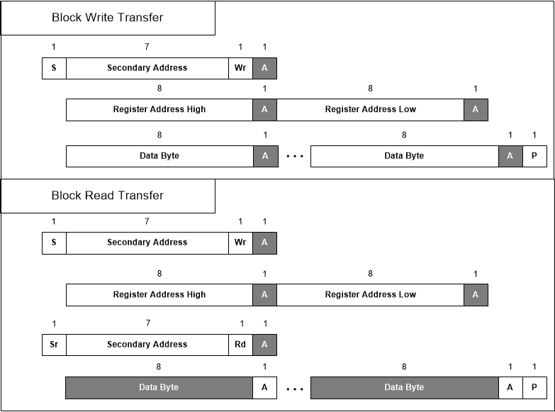
LMK5C23208A I2C Block Register TransfersFigure 8-46 I2C Block Register Transfers