SNVSBU3 March   2021 LP87702

PRODUCTION DATA  

  1. Features
  2. Applications
  3. Description
  4. Revision History
  5. Pin Configuration and Functions
  6. Specifications
    1. 6.1 Absolute Maximum Ratings
    2. 6.2 ESD Ratings
    3. 6.3 Recommended Operating Conditions
    4. 6.4 Thermal Information
    5. 6.5 Electrical Characteristics
    6. 6.6 I2C Serial Bus Timing Parameters
    7. 6.7 Typical Characteristics
  7. Detailed Description
    1. 7.1 Overview
    2. 7.2 Functional Block Diagram
    3. 7.3 Feature Descriptions
      1. 7.3.1  Step-Down DC/DC Converters
        1. 7.3.1.1 Overview
        2. 7.3.1.2 Transition Between PWM and PFM Modes
        3. 7.3.1.3 Buck Converter Load Current Measurement
      2. 7.3.2  Boost Converter
      3. 7.3.3  Spread-Spectrum Mode
      4. 7.3.4  Sync Clock Functionality
      5. 7.3.5  Power-Up
      6. 7.3.6  Buck and Boost Control
        1. 7.3.6.1 Enabling and Disabling Converters
        2. 7.3.6.2 Changing Buck Output Voltage
      7. 7.3.7  Enable and Disable Sequences
      8. 7.3.8  Window Watchdog
      9. 7.3.9  Device Reset Scenarios
      10. 7.3.10 Diagnostics and Protection Features
        1. 7.3.10.1 Voltage Monitorings
        2. 7.3.10.2 Interrupts
        3. 7.3.10.3 Power-Good Information to Interrupt, PG0, and PG1 Pins
          1. 7.3.10.3.1 PGx Pin Gated (Unusual) Mode
          2. 7.3.10.3.2 PGx Pin Operation in Continuous Mode
          3. 7.3.10.3.3 Summary of PG0, PG1 Gated, and Continuous Operating Modes
        4. 7.3.10.4 Warning Interrupts for System Level Diagnostics
          1. 7.3.10.4.1 Output Power Limit
          2. 7.3.10.4.2 Thermal Warning
        5. 7.3.10.5 Protections Causing Converter Disable
          1. 7.3.10.5.1 Short-Circuit and Overload Protection
          2. 7.3.10.5.2 Overvoltage Protection
          3. 7.3.10.5.3 Thermal Shutdown
        6. 7.3.10.6 Protections Causing Device Power Down
          1. 7.3.10.6.1 Undervoltage Lockout
      11. 7.3.11 OTP Error Correction
      12. 7.3.12 Operation of GPO Signals
      13. 7.3.13 Digital Signal Filtering
    4. 7.4 Device Functional Modes
      1. 7.4.1 Modes of Operation
    5. 7.5 Programming
      1. 7.5.1 I2C-Compatible Interface
        1. 7.5.1.1 Data Validity
        2. 7.5.1.2 Start and Stop Conditions
        3. 7.5.1.3 Transferring Data
        4. 7.5.1.4 I2C-Compatible Chip Address
        5. 7.5.1.5 Auto Increment Feature
    6. 7.6 Register Maps
      1. 7.6.1 Register Descriptions
        1. 7.6.1.1 LP8770_map Registers
  8. Application and Implementation
    1. 8.1 Application Information
    2. 8.2 Typical Application
      1. 8.2.1 Design Requirements
      2. 8.2.2 Detailed Design Procedure
        1. 8.2.2.1 Application Components
          1. 8.2.2.1.1 Inductor Selection
          2. 8.2.2.1.2 Buck Input Capacitor Selection
          3. 8.2.2.1.3 Buck Output Capacitor Selection
          4. 8.2.2.1.4 Boost Input Capacitor Selection
          5. 8.2.2.1.5 Boost Output Capacitor Selection
          6. 8.2.2.1.6 Supply Filtering Components
      3. 8.2.3 Current Limit vs Maximum Output Current
      4. 8.2.4 Application Curves
  9. Power Supply Recommendations
  10. 10Layout
    1. 10.1 Layout Guidelines
    2. 10.2 Layout Example
  11. 11Device and Documentation Support
    1. 11.1 Third-Party Products Disclaimer
    2. 11.2 Receiving Notification of Documentation Updates
    3. 11.3 Support Resources
    4. 11.4 Trademarks
    5. 11.5 Electrostatic Discharge Caution
    6. 11.6 Glossary
  12. 12Mechanical, Packaging, and Orderable Information

Package Options

Mechanical Data (Package|Pins)
Thermal pad, mechanical data (Package|Pins)
Orderable Information

Modes of Operation

    SHUTDOWN:The V(VANA) voltage is below the VANAUVLO threshold level or the NRST signal is low. All switch, reference, control, and bias circuitry of the LP87702 device are turned off.
    READ OTP:The main supply voltage (V(VANA)) is above the VANAUVLO level and the NRST signal is high. The converters are disabled and the reference and bias circuitry of the LP87702 are enabled. The OTP bits are loaded to the registers. I2C access is not allowed during OTP read. Section 7.3.8 shows how this also applies to the watchdog.
    STANDBY:The main supply voltage (V(VANA)) is above the VANAUVLO level and the NRST signal is high. All registers can be read or written by the host processor through the system serial interface. Watchdog is active and the WDI input is expected to toggle to avoid watchdog expiration. The converters are disabled and the LP87702's reference, control, and bias circuitry are enabled. The converters can be enabled if needed.
    ACTIVE:The main supply voltage (V(VANA)) is above the VANAUVLO level and the NRST signal is high. At least one converter is enabled. All registers can be read or written by the host processor through the system's serial interface. Watchdog is active and the WDI input is expected to toggle to avoid watchdog expiration.

Figure 7-14 shows the operating modes and transitions between the modes. See Section 7.3.8 for the window watchdog detailed operation.
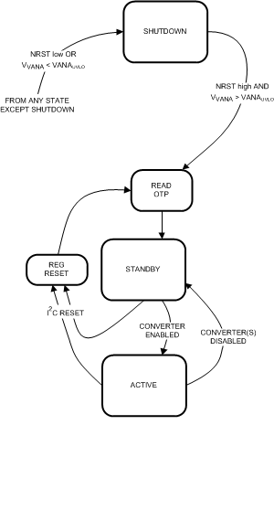
GUID-80E9D20B-3939-43CC-AAFF-D8C9C539399E-low.gifFigure 7-14 Device Operation Modes.