SBOS350B December 2006 – December 2024 OPA4830
PRODUCTION DATA
- 1
- 1 Features
- 2 Applications
- 3 Description
- 4 Related Products
- 5 Pin Configuration and Functions
-
6 Specifications
- 6.1 Absolute Maximum Ratings
- 6.2 ESD Ratings
- 6.3 Recommended Operating Conditions
- 6.4 Thermal Information
- 6.5 Electrical Characteristics VS = ±5V
- 6.6 Electrical Characteristics VS = 5V
- 6.7 Electrical Characteristics VS = 3V
- 6.8 Typical Characteristics: VS = ±5V
- 6.9 Typical Characteristics: VS = ±5V, Differential Configuration
- 6.10 Typical Characteristics: VS = 5V
- 6.11 Typical Characteristics: VS = 5V, Differential Configuration
- 6.12 Typical Characteristics: VS = 3V
- 6.13 Typical Characteristics: VS = 3V, Differential Configuration
- 7 Parameter Measurement Information
-
8 Application and Implementation
- 8.1
Application Information
- 8.1.1 Wideband Voltage-Feedback Operation
- 8.1.2 DC Level-Shifting
- 8.1.3 AC-Coupled Output Video Line Driver
- 8.1.4 Noninverting Amplifier With Reduced Peaking
- 8.1.5 Single-Supply Active Filter
- 8.1.6 Differential Interface Applications
- 8.1.7 DC-Coupled Single-to-Differential Conversion
- 8.1.8 Low-Power, Differential I/O, 4th-Order Active Filter
- 8.1.9 Dual-Channel, Differential ADC Driver
- 8.1.10 Video Line Driving
- 8.1.11 4-Channel DAC Transimpedance Amplifier
- 8.1.12 Operating Suggestions: Optimizing Resistor Values
- 8.1.13 Bandwidth vs Gain: Noninverting Operation
- 8.1.14 Inverting Amplifier Operation
- 8.1.15 Output Current and Voltages
- 8.1.16 Driving Capacitive Loads
- 8.1.17 Distortion Performance
- 8.1.18 Noise Performance
- 8.1.19 DC Accuracy and Offset Control
- 8.2 Power Supply Recommendations
- 8.3 Layout
- 8.1
Application Information
- 9 Device and Documentation Support
- 10Revision History
- 11Mechanical, Packaging, and Orderable Information
Package Options
Refer to the PDF data sheet for device specific package drawings
Mechanical Data (Package|Pins)
- PW|14
Thermal pad, mechanical data (Package|Pins)
Orderable Information
8.1.8 Low-Power, Differential I/O, 4th-Order Active Filter
The OPA4830 can give a very capable gain block for active filters. The quad design lends a very well to differential active filters. Where the filter topology is looking for a simple gain function to implement the filter, the noninverting configuration is preferred to isolate the filter elements from the gain elements in the design. See Figure 8-12 for an example of a 10MHz, 4th-order Butterworth, low-pass Sallen-Key filter. The design places the higher Q stage first to allow the lower Q 2nd stage to roll off the peaked noise of the first stage. The resistor values have been adjusted slightly to account for the amplifier group delay.
 Figure 8-12 Low-Power, Differential I/O,
4th-Order Butterworth Active Filter
Figure 8-12 Low-Power, Differential I/O,
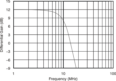
4th-Order Butterworth Active FilterWhile this circuit is bipolar, using ±5V supplies, can easily be adapted to single-supply operation. This configuration adds two real zeroes in the response, transforming this circuit into a bandpass. The frequency response for the filter of Figure 8-12 is illustrated in Figure 8-13.
 Figure 8-13 Differential 4th-Order, 10MHz
Butterworth Filter